Try before you decide on permanent usage of line filter. I made it as a module I can plug directly into AC socket of the DAC and each time I tried it, I never liked it. So I'm not using any line filter, but my mains are rather clean.
Are you looking for that ype of regulator filter http://www.diyaudio.com/forums/showthread.php?s=&threadid=26930&highlight=
Are you looking for that ype of regulator filter http://www.diyaudio.com/forums/showthread.php?s=&threadid=26930&highlight=
This design is more complicated than I thought. Instead of making pictures, you should put it together ")
It looked much simpler here:
It looked much simpler here:
An externally hosted image should be here but it was not working when we last tested it.
mikelm said:Not sure that I agree.
It just looks as if BrianGT has two boards next to each other - otherwise they look quite alike.
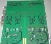
BrianGT - Why have you got two boards together like that ? is it to do with costs ?
Peter - how come you manage to post full size pictures ?
mike
Mike,
They were put on a single pcb to save costs. The pcb will be cut apart to create 2 seperate boards. These are prototype boards with 2 different grounding topologies. I will make another 2 boards after Peter and I see how these work.
As for the picture posting, if you load the picture on a website outside the forum, you can post a direct IMG link, which will cause it to appear on the site. It looks like Peter is using some polish site for hosting that image.
/brian
Thanks for the link Elso. Are you still using pi-filter mentioned therein?
"Try before you decide on permanent usage of line filter. I made it as a module I can plug directly into AC socket of the DAC and each time I tried it, I never liked it."
What didn't you like? Rounding of transient edges? Reduction in dynamics?
"So I'm not using any line filter, but my mains are rather clean."
That is a rather fortunate situation for an audiophile. My mains has a continuous series of peaks and noises at a wide variety of frequencies.
The Schaffner line filter I use provides 25db attenuation at 10kHz, 80dB at 100kHz, 80dB at 1MHz, and 63dB at 10Mhz, while generating some noise of its own at higher frequences. I am familiar with the sonic disadvantages it brings, but, in my situation, it is better to have a common-mode choke-coil-based AC power line EMI suppressor than not. I have been planning of building a discrete lien filter using the attractive Murata PLA10 Series with the "sectional winding technique," since it pushes the insertion loss a bit higher in frequency
"Are you looking for that type of regulator filter?"
No, but thanks for the picture. My main problem with T-networks in this 3D DAC layout is the size and pin configuration: T-Networks are designed for pcb placement, but I want to mount the pre-regulator filter directly onto the pins of a TO-92 case reg. My typical pre-regulator filter will not work here without bending the Vout pin rather severely to avoid a short. Does anyone know a suitable pre-regulator filter for TO-92? I think it would also be possible (as a plan B) to build a discrete pre-reg filter with one or two caps, an SMD choke, and an SMD resistor, but I would like to hear opinions before I jump into it. I am worried that this will create more problems than solve.
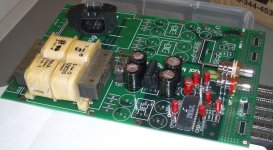
Brian, nice pcb. But I would mainly be interested in the part where the PSU is located... and leave the rest for 3D p-to-p. Perhaps two separate boards, to leave the p-to-p option open. The two could be stacked in order to save space.
Best regards
"Try before you decide on permanent usage of line filter. I made it as a module I can plug directly into AC socket of the DAC and each time I tried it, I never liked it."
What didn't you like? Rounding of transient edges? Reduction in dynamics?
"So I'm not using any line filter, but my mains are rather clean."
That is a rather fortunate situation for an audiophile. My mains has a continuous series of peaks and noises at a wide variety of frequencies.
The Schaffner line filter I use provides 25db attenuation at 10kHz, 80dB at 100kHz, 80dB at 1MHz, and 63dB at 10Mhz, while generating some noise of its own at higher frequences. I am familiar with the sonic disadvantages it brings, but, in my situation, it is better to have a common-mode choke-coil-based AC power line EMI suppressor than not. I have been planning of building a discrete lien filter using the attractive Murata PLA10 Series with the "sectional winding technique," since it pushes the insertion loss a bit higher in frequency
"Are you looking for that type of regulator filter?"
No, but thanks for the picture. My main problem with T-networks in this 3D DAC layout is the size and pin configuration: T-Networks are designed for pcb placement, but I want to mount the pre-regulator filter directly onto the pins of a TO-92 case reg. My typical pre-regulator filter will not work here without bending the Vout pin rather severely to avoid a short. Does anyone know a suitable pre-regulator filter for TO-92? I think it would also be possible (as a plan B) to build a discrete pre-reg filter with one or two caps, an SMD choke, and an SMD resistor, but I would like to hear opinions before I jump into it. I am worried that this will create more problems than solve.
Brian, nice pcb. But I would mainly be interested in the part where the PSU is located... and leave the rest for 3D p-to-p. Perhaps two separate boards, to leave the p-to-p option open. The two could be stacked in order to save space.
Best regards
Cut apart???
"They were put on a single pcb to save costs. The pcb will be cut apart to create 2 seperate boards. These are prototype boards with 2 different grounding topologies. I will make another 2 boards after Peter and I see how these work."
Looking at top view of pcb, me thinks that this is indeed a "double mono pcb" with right channel on one side, and left channel on another. The (partially obscured) printing on the pcb would indicate just that...
Bottom view however does show different ground routes.
slawney said:Cut apart???
"They were put on a single pcb to save costs. The pcb will be cut apart to create 2 seperate boards. These are prototype boards with 2 different grounding topologies. I will make another 2 boards after Peter and I see how these work."
Looking at top view of pcb, me thinks that this is indeed a "double mono pcb" with right channel on one side, and left channel on another. The (partially obscured) printing on the pcb would indicate just that...
Bottom view however does show different ground routes.
The whole dual mono text and a few random traces are just an attempt at making the design look like one board, so that when I get the prototype pcbs made, I don't get charged an extra tooling fee for having 2 designs on one pcb (actually 4 designs if you count the prototyping adapters on the front of the pcb.
The board is mailed up to Peter for testing. I will make my own pcb once he provides me feedback on the design.
--
Brian
slawney said:What didn't you like? Rounding of transient edges? Reduction in dynamics?
The Schaffner line filter I use
Mostly diminishing clarity and adding coloration. I observed the same with ferrites, so I'm not using them either.
I thought you were using batteries?
Some (hopefully) useful tips
With my version of the 3D dac I find the best decoupling to be a 1206 X7R ceramic SMD cap, which just so happen to fit perfectly across two pins on the CS8412.
I'm using 1uF at the moment, following my less is more dogma, but I think 4.7uF sounds just the same.
If you build the 3D layout with a foil groundplane on top of the CS8412, you can solder a 0805 SMD cap directly between the "shelf" of the TDA1543 supply pin and the ground plane. I'm using 100nF, though perhaps a smaller value would be appropriate.
After each LM317 I use a 4700uH/20R inductor from Farnell and no output cap. You need to boost the reg voltage a little compensate for voltage drop and avoid distortion. I'm using 4.7uF 1206 on Vin and ADJ.
I'm trying Panasonic FC 220uF 25V / 1uF 1206 X7R on the CS8412 analog ADJ and it seems to do the business. Note that this combination sounds dreadful decoupling the digital chips, but my AD817 I/V loves it.
Big, lush, dynamic sound.
A bit of experimentation later and I'm using a different LM317T arrangement, which sounds more natural (ie there seems to be less gunk and discoloration in the sound).
Input via 4700uH
ADJ bypassed with 220uf 25v FC / 1uf X7R 1206
Output bypassed with 220uf 25v FC
4700uH on the output
220uF 25v FC local decoupling
Input via 4700uH
ADJ bypassed with 220uf 25v FC / 1uf X7R 1206
Output bypassed with 220uf 25v FC
4700uH on the output
220uF 25v FC local decoupling
An externally hosted image should be here but it was not working when we last tested it.
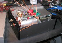
Here's my latest implementation of 3D TDA1543 DAC. The following changes has been done with regards to a previous version:
I'm using now 2 smaller 12V YUASA cells. They are somewhat cleaner sounding than Panasonics, with better vocal presence. There isn't ANY ceramic bypasses anymore, and not any small bypasses before regulators.
I'm using 47/50 BG N after each battery and on the DAC chip. I found that this cap sounds much better than 100/16 BG N I was using previously (also for battery bypass this seems like a best choice).
I tried briefly Scientific Conversion input transformer, and although fine sounding, it possesed slight coloration I couldn't get used to. Presently, I'm using Neutrik BNC, 75 Caddock after (best choice resistor type, IMO) and 2 Vishay/ERO coupling caps. Those caps are very neutral and transparent in this application (my thanks to Klaus for raving so much about them
).Still, the same input driver, but with 15/20 OsCon for bypass. There is also ferrite bead before regulator here and one more OsCon. This was the only area in a circuit that I actually preferred OsCons.
The receiver has BG 10/50 N type for bypasses and anoter ferrite bead before digital section regulator. The ferrite bead does not sound good on analog side.
PLL filter consists of 0.47 BG NX and 400R Caddock and additionally 3n3 Wima cap. I also tried 4.7 BG N and 100R resistor but this created too much emphasis on the midrange and I regard the other choice as overall better tonal balance.
I'm still using RIkens for I/V but will try Caddocks TF020 soon. I had BG N 4.7 caps for coupling initially, and they worked great, but after switching to Siemens MKV 3u3, there is no coming back. They just provide another level of refinement with better resolution and bass definition.
That's about all for that version. I've been working on that DAC for almost a year, and I don't think anything can be improved much. I'm positively sure that PASSIVE I/V IS better to active and reclocking is not needed. Batteries bring another level of performance and ARE better than AC power (more clarity)
This DAC is also better at the moment as the parallel TDA1541S2 DAC that I tweaked recently. But I believe if similar approach is taken to pushing the envelope of TDA1541 DAC, much more improvement is still expected and maybe even a superior performance
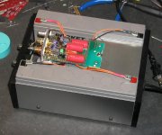
So I decided to make a permanenet DAC enclosure, implementing open chassis (design) as well as battery power, with a built in charger and vibration free structure.
The charger (one per battery), is based on two LM317 regulators, 12VA transformer and it's placed in 3 x 2 tubing at the back of a chassis.
The base is made of 3/4 maple board, two thin aluminum angles make the sides, and two more acrylic panels create front and a back.
The charger (one per battery), is based on two LM317 regulators, 12VA transformer and it's placed in 3 x 2 tubing at the back of a chassis.
The base is made of 3/4 maple board, two thin aluminum angles make the sides, and two more acrylic panels create front and a back.
Attachments
The Siemens MKV caps are freely placed at the bottom, the DAC board is loosely fited with 2 screws located on a charger enclosure, the other end supported by soft ruber rests on the capacitors. The switch disconnects the chargers and allows battery only use.
Attachments
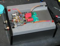
Hi, It is funny to see how Peter and I have gone in totally different directions starting with the same DAC (TDA1543). I am using active IV-conversion with OPA627BP, discrete outputbuffer, opamp regulated analog powersupply and a huge 100Watt(!) transformer.
Peter what are those Siemens MKVs for?
Peter what are those Siemens MKVs for?
Elso Kwak said:Hi, It is funny to see how Peter and I have gone in totally different directions starting with the same DAC (TDA1543). I am using active IV-conversion with OPA627BP, discrete outputbuffer, opamp regulated analog powersupply and a huge 100Watt(!) transformer.
Peter what are those Siemens MKVs for?
Did you post the schematic anywhere or is it "personal"? I'd like to switch my TDA1543 DAC to active I/V...
Re: Re: The ultimate TDA1543 DAC layout??
Hi UrSv,
Only the discrete outputbuffer is "personal" though I think the correct English term is proprietary. The buffer is similar though to Sonnya's one here:
http://www.diyaudio.com/forums/showthread.php?s=&threadid=1794&highlight=sonnya+cascode
In the past I posted a regulated supply with a triple Darlington for the TDA1543, the opamp regulated analog supply, and the IV and outputbuffer/ low-pass filter general schematic. Also I posted the DIR with the AD8561 in front, Wildmonkeysects’ loop-filter.
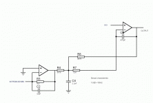
In the picture ??= ground.
The non-inverting input of the first opamp is connected to Vref of the DAC with 3k3 to ground . R3 = 3k65 and C2= 3n3 with IN from the TDA1543. First opamp OPA627BP, second opamp the discrete. Not shown 0.47µF Audionote PIO copper foil output caps.
UrSv said:
Did you post the schematic anywhere or is it "personal"? I'd like to switch my TDA1543 DAC to active I/V...
Hi UrSv,
Only the discrete outputbuffer is "personal" though I think the correct English term is proprietary. The buffer is similar though to Sonnya's one here:
http://www.diyaudio.com/forums/showthread.php?s=&threadid=1794&highlight=sonnya+cascode
In the past I posted a regulated supply with a triple Darlington for the TDA1543, the opamp regulated analog supply, and the IV and outputbuffer/ low-pass filter general schematic. Also I posted the DIR with the AD8561 in front, Wildmonkeysects’ loop-filter.
In the picture ??= ground.
The non-inverting input of the first opamp is connected to Vref of the DAC with 3k3 to ground . R3 = 3k65 and C2= 3n3 with IN from the TDA1543. First opamp OPA627BP, second opamp the discrete. Not shown 0.47µF Audionote PIO copper foil output caps.
Attachments
- Status
- This old topic is closed. If you want to reopen this topic, contact a moderator using the "Report Post" button.
- Home
- Source & Line
- Digital Source
- The ultimate TDA1543 DAC layout??