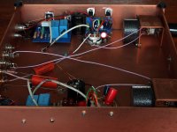
As per Salas, suggest move input J1 to lower edge of brd about midpoint (roughly below the present R13) Will probably need to increase the "vertical" distance (height?)
At the same time, consider using that vacant area between the Q1 and Q4 as a convenient point for the output pins (it doesn't have to be a traditional +/- connector at all) and so the 0volts points are neatly together at the bottom edge of the pcb - will also need to move the R12 + C3, unfortunately.
Random other thoughts - R15 could fit neatly between Q2,Q9 and, D1 could do with a cap across it (IMO, that is) and the "Jsense" point is a bit confusing.
Perhaps, also move the resistors R4, R5 a bit further away from the Fet pins and you might consider adding the option to connect the R6 closer to the central 0volt point rather than directly to the Fet - not sure if any advantage, but just another donut
This will give a more compact, shorter track version but the "more square" board may not suit your requirements.
None of these comments may be of any use to you, and it's good to see your design - good fun, this!
my 2 cents ...
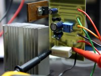
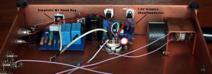
Thanks Salas and James for the help. The general board shape is important for my final configuration, but, I can adjust other items. The Jsense is for a a socket with two legs filed off. The first board will be used in a prototype, so, I expect to be connecting and disconecting frequently and don't want to desolder all the time.
Ken
Attachments
...strange the link not work for me ....
It is strange... links like that rarely seem to work for me either - maybe it's because I have my page size set to 50 and the link is posting to page # / maybe not. Perhaps a forum wizard can shed some light on it.
Hi,
when the link is direct to the post, then you are taken to that post irrespective of what your page setting is.
There seems to be some other way to generate a link and this does some kind of arithmetic using the default page size and takes one to the correct post only if the reader uses default page size.
I too have my page set to 50 and most links work. The occasional link goes to much earlier due to that arithmetic I referred to.
I will post this in Forum Problems.
Salas, my fault this is the wrong forum.
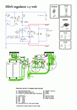
Was just searching on Digikey for an adjustable reg for the dc heater portion of the SSHV, QH specified lt1084 and said that ld was interchangeable.
I'll put on QH thread next time around.
Thanks
You posted the wrong place!
well every linear tech drop in replacement I have used has been superior and not just for dropout spec. usually lower ripple/noise and better dynamic load regulation. LT317/337 vs. LM317/337 is a good example.
so anyway how is development of the PCB going? has the prototype been recieved yet? suppose i'll go check the GB thread hehe
so anyway how is development of the PCB going? has the prototype been recieved yet? suppose i'll go check the GB thread hehe
Hi Salas,
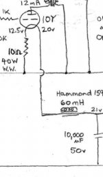
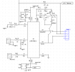
At the risk of being heckled again, I have a question about decoupling caps at the load. In this case my "load" is an LME49811. As I was reading Iko's thread, I seem to remember Bill mentioned that he is implementing the regulators without decoupling caps. Did I get this right? Should there be any decoupling caps?
If no caps, what does the ground connect to? I currently run this device with the signal grounds separate from the power grounds (schematic attached). Would I continue with this grounding arrangement (just omit the decoupling)? As you can see there is one point on the chip for a ground connection, I believe that this is a power ground connection.
Thanks for your help.
Ken
Attachments
- Status
- This old topic is closed. If you want to reopen this topic, contact a moderator using the "Report Post" button.
- Home
- Amplifiers
- Power Supplies
- The simplistic Salas low voltage shunt regulator