The stereo image doesn't seem to me like it has that "out of phase phase" central suckout though. What made you think so?
It is precisely that "out of phase central suckout" feeling...
I couldn't really believe it either, so I double checked, rather unscientifically I must admit: I did open the files in Audacity, and when mixing down the channels to mono, I got a much louder resulting mono file when inverting one of the channels...
I fixed the sample files, just by inverting the right channel in Audacity.
RJM Audio recording folder
I love analog ... but its times like these that I really love digital too!
RJM Audio recording folder
I love analog ... but its times like these that I really love digital too!
Happy to help! [emoji2]Well, you're da man CHiroshi! I found that R channel was wired inverted in the headshell.
(which was my fault of course .... I must have spaced out last time I replaced my cartridge.)
Other than that I couldn't hear a difference between the two... Listening through a TC electronic konnekt 8 audio interface and my Beyerdynamic D770.
It is honestly very hard to hear a difference, and you matched the levels on the different files really well!
If anything I might sort of find the phonoclone 3.5 a tad crispier, especially listening to the hi-hat and the strings. The crystalFET, I might feel it has a bit more presence in the lower register (bass guitar).
All the above compared to he phonoclone 4.0... which I, in the other hand, don't find lacking in any way...
Fancy throwing a VSPS in the comparison?..")
If anything I might sort of find the phonoclone 3.5 a tad crispier, especially listening to the hi-hat and the strings. The crystalFET, I might feel it has a bit more presence in the lower register (bass guitar).
All the above compared to he phonoclone 4.0... which I, in the other hand, don't find lacking in any way...
Fancy throwing a VSPS in the comparison?..
I found the 4.0 and CrystalFET extremely close, which surprised me. (The CrystalFET was recorded at +6 dB as the native gain is only 50~52 dB, all three recordings were made through the SapphirePre for analog level control) The 3.5 stands out as being drier.
As an aside, as a tool I'm finding this exercise invaluable. It may not be a perfect recording, but whatever degradation creeps in over the A-D-A conversion pales in comparison to the ability to listen back and forth instantly and repeatedly until you can be satisfied you are really hearing what you think you are.
No can do on the VSPS - I haven't owned a MM cartridge in years, so I don't have one.
phonoclone 4.0b final report
Time to wrap this up.
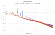
With the standard unregulated supply there is more ripple noise in the output of the Phonoclone4 (pc40b) than the previous version phonoclone 3.5h, or the CrystalFET. This additional noise, while measurable above the broadband baseline, does not produce any discernible effect on the sound quality. Furthermore, it can be eliminated entirely by using a regulated power supply. (I used a Z-Reg board mounted inside the external supply.)
The ripple noise is coupled to the input section of the phonoclone from the unregulated voltage (V++, V--) not the output of the S-Reg regulator section (V+) or the ground (COM). The S-Reg is cleaning up the V+,V- rails just fine, but insufficient shielding and/or spacing between the unregulated supply
and the phonoclone input leads to ripple in the output signal regardless. This was verified by removing C6,7 from the circuit which would be expected to increase the ripple on V+,V- about 10 times and observing that the output ripple noise was unaffected.
I do not know why the pc40b with the S-Reg has substantially higher ripple noise than the X-Reg based pc35h, but I note that the CrystalFET has a similar signal though much smaller. It could be related to board layout, or be fundamental to the S-Reg circuit, or both.
Finally I should report two issues I encountered that made testing and analysis difficult: one is that the connecting cable between power supply and phonoclone, with the Z-Reg at the power supply end, oscillated badly when there was no ceramic capacitor on the Z-Reg output. So caution is needed when using a regulated supply - the result can be worse than unregulated. Second, more obvious, is that the bench measurements tended to show more noise than what I observed when installed in the audio system. This related to the dummy resistors used on the phonoclone inputs, and the length of connecting wires at the inputs, and testing with the cover on or off. It's easy to get led astray measuring changes to noises that don't exist except as interference on the bench test setup.
So that's it: I like the Phonoclone 4. A lot actually. I will use mine with a standard unregulated power supply as per the BOM. There is more hum with the volume turned full up than my other designs however. A regulated power supply will solve this. I do not know how to reduce the ripple noise further while still using an unregulated supply, but it is a matter of separation, isolation, and shielding - exactly what and how much is required is left for future work.
Time to wrap this up.
With the standard unregulated supply there is more ripple noise in the output of the Phonoclone4 (pc40b) than the previous version phonoclone 3.5h, or the CrystalFET. This additional noise, while measurable above the broadband baseline, does not produce any discernible effect on the sound quality. Furthermore, it can be eliminated entirely by using a regulated power supply. (I used a Z-Reg board mounted inside the external supply.)
The ripple noise is coupled to the input section of the phonoclone from the unregulated voltage (V++, V--) not the output of the S-Reg regulator section (V+) or the ground (COM). The S-Reg is cleaning up the V+,V- rails just fine, but insufficient shielding and/or spacing between the unregulated supply
and the phonoclone input leads to ripple in the output signal regardless. This was verified by removing C6,7 from the circuit which would be expected to increase the ripple on V+,V- about 10 times and observing that the output ripple noise was unaffected.
I do not know why the pc40b with the S-Reg has substantially higher ripple noise than the X-Reg based pc35h, but I note that the CrystalFET has a similar signal though much smaller. It could be related to board layout, or be fundamental to the S-Reg circuit, or both.
Finally I should report two issues I encountered that made testing and analysis difficult: one is that the connecting cable between power supply and phonoclone, with the Z-Reg at the power supply end, oscillated badly when there was no ceramic capacitor on the Z-Reg output. So caution is needed when using a regulated supply - the result can be worse than unregulated. Second, more obvious, is that the bench measurements tended to show more noise than what I observed when installed in the audio system. This related to the dummy resistors used on the phonoclone inputs, and the length of connecting wires at the inputs, and testing with the cover on or off. It's easy to get led astray measuring changes to noises that don't exist except as interference on the bench test setup.
So that's it: I like the Phonoclone 4. A lot actually. I will use mine with a standard unregulated power supply as per the BOM. There is more hum with the volume turned full up than my other designs however. A regulated power supply will solve this. I do not know how to reduce the ripple noise further while still using an unregulated supply, but it is a matter of separation, isolation, and shielding - exactly what and how much is required is left for future work.
Attachments
Grounding layouts part II (revised)
I've been studying op amp grounding techniques and revised my ideas on the subject somewhat.
There are two basic approaches, single point and ground plane. For audio frequencies single point is considered more appropriate, though often mixed with a partial ground plane. Single point is as the name implies - all the returns are tied together a at a common point. The most rigorous version of this idea is called "star grounding" but often what you'll see is the inverting inputs, noninverting inputs, outputs, and power supply each bundled together first in a group before joining to each other.
The problem with rigorous star grounding is that closed loop op amp bandwidth can even for audio projects be up in the region where ground plane techniques would actually have some merit, i.e. the inductance of individual traces starts to be important. Star grounding involves many more long traces than a ground plane, and this can cause problems. A hybrid approach can be something of a best-of-both solution.
The textbook book advice you'll easily find from any web search is simple enough: bypass close to the op amp power pins, avoid daisy chaining grounds, and make current loops as small a possible. Finding a reliable example showing how to do it right is much harder however. The attached pdf from Power Amp Design is the best - most relevant anyway - documentation I could snag on the subject.
The basic point that confuses me is "where exactly is the reference ground point that everything must return to?"
The best answer I can give with my present understanding of the subject is the op amp's positive and/or negative power pins and by direct extension the area of the ground trace the bypass capacitors connect to.
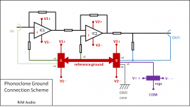
That's where you start, and of course with two op amps like the phonoclone has that means there are two reference points (A and B in the figure) physically separate. These should be as soundly joined as possible, and also - and this is the part I didn't properly appreciate before - only the bypass current should be allowed to flow through this region. The load current, which flows from OUT- ultimately back to COM, should be kept out so as to avoid polluting the reference and thus mixing up with the inputs and causing a ground loop.
So as far as the reference ground goes that means the inputs of IC1 connect back to A, the inputs of IC2 connect to somewhere in the middle, and the COM and OUT- are jointed together at the opposite side of B. I'm still not 100% confident about where the best place for the case connection is, A or B, but I've shown it at B next to the OUT- and COM. It shouldn't matter if everything works as advertised such that no load currents flow in the reference.
That's a formal scheme developed for a power op amp chip. A line level circuit like the phonoclone or VSPS should not be nearly as sensitive to load currents as they are so much smaller, but it must be said that phonoclone 3.5h layout followed this arrangement more rigorously than the 3.8 and 4.0b layouts where the COM and OUT- were placed at opposite sides of the board with the bypass caps in between. What that amounts to in the diagram below is connecting OUT- at A rather than B.
As well as all the above consideration, there is still the matter of current loop area to be considered, though in looking over my previous layouts there's nothing there which is terrible in this respect. Loops are generally pretty small. Also, the bypassing arrangement should be fine for the op amp bandwidths in the RJM phono stages, which is only about 300 kHz.
I've been studying op amp grounding techniques and revised my ideas on the subject somewhat.
There are two basic approaches, single point and ground plane. For audio frequencies single point is considered more appropriate, though often mixed with a partial ground plane. Single point is as the name implies - all the returns are tied together a at a common point. The most rigorous version of this idea is called "star grounding" but often what you'll see is the inverting inputs, noninverting inputs, outputs, and power supply each bundled together first in a group before joining to each other.
The problem with rigorous star grounding is that closed loop op amp bandwidth can even for audio projects be up in the region where ground plane techniques would actually have some merit, i.e. the inductance of individual traces starts to be important. Star grounding involves many more long traces than a ground plane, and this can cause problems. A hybrid approach can be something of a best-of-both solution.
The textbook book advice you'll easily find from any web search is simple enough: bypass close to the op amp power pins, avoid daisy chaining grounds, and make current loops as small a possible. Finding a reliable example showing how to do it right is much harder however. The attached pdf from Power Amp Design is the best - most relevant anyway - documentation I could snag on the subject.
The basic point that confuses me is "where exactly is the reference ground point that everything must return to?"
The best answer I can give with my present understanding of the subject is the op amp's positive and/or negative power pins and by direct extension the area of the ground trace the bypass capacitors connect to.
That's where you start, and of course with two op amps like the phonoclone has that means there are two reference points (A and B in the figure) physically separate. These should be as soundly joined as possible, and also - and this is the part I didn't properly appreciate before - only the bypass current should be allowed to flow through this region. The load current, which flows from OUT- ultimately back to COM, should be kept out so as to avoid polluting the reference and thus mixing up with the inputs and causing a ground loop.
So as far as the reference ground goes that means the inputs of IC1 connect back to A, the inputs of IC2 connect to somewhere in the middle, and the COM and OUT- are jointed together at the opposite side of B. I'm still not 100% confident about where the best place for the case connection is, A or B, but I've shown it at B next to the OUT- and COM. It shouldn't matter if everything works as advertised such that no load currents flow in the reference.
That's a formal scheme developed for a power op amp chip. A line level circuit like the phonoclone or VSPS should not be nearly as sensitive to load currents as they are so much smaller, but it must be said that phonoclone 3.5h layout followed this arrangement more rigorously than the 3.8 and 4.0b layouts where the COM and OUT- were placed at opposite sides of the board with the bypass caps in between. What that amounts to in the diagram below is connecting OUT- at A rather than B.
As well as all the above consideration, there is still the matter of current loop area to be considered, though in looking over my previous layouts there's nothing there which is terrible in this respect. Loops are generally pretty small. Also, the bypassing arrangement should be fine for the op amp bandwidths in the RJM phono stages, which is only about 300 kHz.
Attachments
Last edited:
bench notes:
re-wiring out- and the return or R8 to the other side of the bypass caps on phonoclone 4.0b does not change the output ripple, -78 dB at 120 Hz.
adding a mu-metal screen between the S-Reg and phonoclone parts of the circuit does not change the output ripple.
The output ripple is the same level in both channels. Although obscured by broadband noise, it resembles an inverted triangle wave i.e. originating from the negative rail rather than the positive.
Attachments
back to square one
AN-202 "An IC Amplifier User’s Guide to Decoupling, Grounding, and Making Things Go Right for a Change" By Paul Brokaw was my main reference back when I first started doing op amp board layouts.
The phonoclone 3.5h boards rigorously follow Fig. 10 of the AD app note. Thing is, all my layouts do, and if the 4.0b layout makes a small concession to use a full ground plane, I already checked that wiring it rigorously starred does not change matters.
What is the quote? "I've done nothin' wrong, guv!" I concede it might be a layout problem, but it is not a ground loop problem as far as I can tell.
What else do I know for sure? Well, that the noise is picked up at the input of IC1, i.e. that it manifests itself as a potential difference between the inverting and noninverting terminals of IC1. I know that the noise is rectified power line harmonics, and I know that the noise originates in the voltage regulator, and I know that the noise appears not to be transmitted over free space or picked up by the input wiring but is instead coupled at the board level.
Which you'd think would be enough to ID the problem but alas I am stumped.
Attachments
Last edited:
have a look at figures 3 a,b,c.
he has analysed the CURRENT routes. In each case the LOOP AREA must be minimised to minimise the susceptibility to emi (interference).
Now look at fig 9.
Analyse that for CURRENT in the input circuit and in the output circuit.
Then remove the shared route and minimise LOOP AREAs.
I think you need to apply the same logic to your PCB layout.
If any current route needs to pass very high frequencies, then it is not sufficient to minimise loop area, one must also minimise loop inductance (loop impedance).
Last edited:
Andrew,
You are right, in addition to the connection order of the returns, there is also a matter of loop area. The bigger the loop, the bigger the receiving or transmitting antenna. Loop area is frequency dependent, at high frequencies the bypass capacitors are effective and generally work to drastically reduce loop area, at low frequencies the loop usually goes back to the power supply or at least the filter capacitors.
I believe there is a rule about antennas in that the antenna length has to be larger to work at low frequencies. I don't think anything at the board level is going to act as an antenna for 120 Hz.
Correct me if I'm wrong there though.
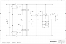
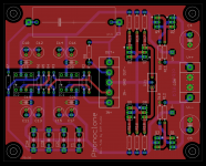
This is my latest layout for the phonoclone 4. I'm not really convinced this would make any difference, but it addresses the following two concerns:
The return connection is rigorous and centralized like it is in pc35h. In particular the S-reg output section Q5-8 and R21 are connected to the reference directly with a dedicated trace.
The V+ and V- planes are replaced with traces. I'm ambivalent, but the argument goes that having the voltage rails spread out over a wide area increases likelihood of noise coupling to the input.
Residual concern is inverting and non-inverting traces run on top of each other on opposite sides of the board. Generally you want them physically separated.
Attachments
Most circuits draw alternate currents from the +ve and -ve supply rails. Whether the +ve is flowing, or the -ve is flowing, during any halfwaveform, the return circuit must be included in the Loop analysis.
If one places the Return next to the +ve current route to help minimise interference, then one MUST also move the -ve to run along side the Return to minimise Loop area.
It's this requirement to have both the +ve and -ve current supplies next to the Return that makes for good emi performance.
And it's exactly the same reason that makes the twisted triplet for the PSU to circuit power supply cable a necessity.
Granted, but EFI/EMI isn't so much the problem: ripple is. Ripple transmitted from the regulator and/or environs to the input section by methods unclear.
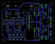
Layout 43h improves the ground plane coverage and puts all the signal traces on the bottom layer with the inverting and noninverting well separated.
The only downside here is a couple of instances where the noninverting signal traces duck under the V+ and V-. As for loops - the ground plane ensures current loops are minimized, at least inductively.
Attachments
Ripple is a current variation. Ripple is interference !but EFI/EMI isn't so much the problem: ripple is.
But how does this interference get into the input signal? How is it that it interferes? The physics I can grasp. What I can't figure out is the specifics relating to the board layout: the "this loop here radiates and is picked up by that loop there..." of it.
*****
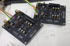
A big delivery of boards arrived this morning, including the new VSPS200m pictured. The quality from pcbcart continues to improve, with polished edges, high resolution printing, and a thick matte finish... nicest boards I've yet handled.
*****
A big delivery of boards arrived this morning, including the new VSPS200m pictured. The quality from pcbcart continues to improve, with polished edges, high resolution printing, and a thick matte finish... nicest boards I've yet handled.
Attachments
- Home
- Source & Line
- Analogue Source
- The Phonoclone and VSPS PCB Help Desk