I agrre with Tekko! You can just begin with a simple full bridge design with mosfet drivers for power stage..That's work great if you use TC4420 and TC4429 drivers with only 1 drive signal from lM319....You get a schematic right now! That's the simple class d you can built! At 18V you can get 40W into 4 ohms....
Fredos
www.d-amp.com
Fredos
www.d-amp.com
Tekko, he's into pro audio, and copies the design from the Chinese, as they have identical looking products 
Fredos, pretty cool of you to be giving out those kinds of hints on your newest Chinese rip off. I think the idea of a seperate charge pump is well served. Drivers have been using it for awhile, at least I thought so? I wonder why it isn't implemented more commonly or as default with the standard higher power driver IC's.
I like how you take care of clipping as well, very nice.
Good luck with em. Sorry for the chinese rip off joke.. I'm just beyond help.
Thanks classd4sure!
Anyways, I'm working now on news approach with combinated power amp and switching power supply, in phase modulation schem, all IGBT power converter. I have fews bug to fix, but so fare 2kW of power continuously without heat sink on booth switching device and output device...All surface mount! Sound is bit harsh for now, but I work hardly on this!
More info now...The circuit is a reference switching power supply without rectifier diode. 4 AC switch with IGBT switch the reference signal (2 in 45 degree phase and 2 in 270 phase) to a low pass filter and PWM signal control the phase between 0-90 degree and 180-360 degree for other leg. Work weel for now, stable, VERY efficient, but sound is bit harsh, I have to found why...Each part work at 125kHz, but PWM at output filter is 250Khz, because reference switch in the midle of the sequence of the AC switch. Effective frequency is 500kHz because we run power signal in differential mode....Some pick of the prototype soon! Very simple and efficient!
If someone have evre built a power converter like this and have experience, let me know!
Sleep time...!
Fredos
www.d-amp.com
Sorry Tekko...
Yes I design and built amplifier for fun, but the more funny thing is that now I can live with this!
Thanks for comment!
Fredos
www.d-amp.com
Yes I design and built amplifier for fun, but the more funny thing is that now I can live with this!
Thanks for comment!
Fredos
www.d-amp.com
Do you really believe what you write?
Your pictures clearly show mains rectification diodes, rectified mains storage capacitors, two IGBTs in half-bridge configuration, DC blocking capacitors for the transformer, output rectifier diodes without any filter (the supply is either badly or not regulated) and output storage capacitors.
Why telling fairy tales about rectifierless supplies, a pair of SMD IGBTs without heatsink producing 2KW continuous in half bridge at 125Khz and the like? Each IGBT would be dissipating over 100W in these circumstances (and I know because I'm tired of using them).
Obviously you are taking advantage of the fact that most people reading your thread has never designed and built switching mode power supplies, but I have been doing that for quite a long time now, so you can't just deceive me. I'm sorry (not to mention that now I'm applying all that switching experience to class D).
Finally, if you want to reduce the "harsh sound" problems, you'll have to take an oscilloscope and start finding and fixing switching glitches on every circuit node. You'll probably have plenty of them judging by what you told, and they disturb op-amps and comparators quite badly
p.s. You have not explained us yet how do you expect to reduce or prevent MOSFET body diode conduction by paralleling an external diode whose voltage drop is way higher than the voltage drop from the own body diode. That's only possible when you don't bother reading the datasheets!! The fact speaks for itself.
Why did you seem so puzzled when I mentioned diode charge storage phenomena? That's elemental PN junction semiconductor theory!! Stored charge is a key parameter that determines reverse recovery time and reverse peak current.
Also, that sentence about some comparator hysteresis increasing as instantaneous input signal level increases is even funnier, because it has to be exactly the opposite in order to obtain a relatively stable operating frequency.
Take classd4sure's advice and tell us what are you trying to copy
Eva!
That's a different design. The rectifiers he mentioned are not on mains, but after the transformator. But whatever it is, it is unbelieveable.
fredos writes "continuous", but he states on his homepage that "In the case that measurement are done with the non significant method of continuous sine wave input signals (applied for more than 30 seconds), the system is self-protected from that unusefull signals, and lower output values will be found."
Some confusing issues here and we all struggle with the typical language barrier at times.
Firstly we have the ES1D? diode mentioned to be in "anti parallel".
I've heard of anti series in this application, but from the context of everything else it seems this diode would be in parallel would it not?
Secondly EVA speaks to recombination time without any added reverse polarity, natural recombination, this can be sped up with added reverse polarity, but then.... you have high EMI, it would seem.
Fredos mentions using it for it's faster application.. and then the body diode takes over. So can you further explain the usefullness of the // diode if the body diode still conducts for the majority of the time? Am rather confused here, it's a complex topic and can't be discussed very well in bits and pieces like this.
Lastly, Fredos also rates his amps in apparent power, which is only relevant from the point of view of the SMPS capability, and not what it produces across the load, it would seem.
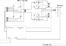
Also, if anybody tries to count SMPS transformer turns ratio, the result will be something like 35:7+7. That in turn will produce +-32V rails in a half bridge configuration, and +-64V if I'm wrong and there are two more IGBTs not shown in the picture to form a full bridge. Anyway, the power output attainable with these rails is clearly lower that the ratings claimed, as in practice +-64V unregulated at no load won't produce much more than 400W on 4 ohms!!
If the mains was not being rectified directly, why there are three or more clear-blue coloured big storage capacitors on the left side of the picture with a heatsink near them? It's too obvious that a mains diode bridge is mounted on that heatsink. Also, the classic NTC inrush supressor routinely employed in that arrangement is clearly shown in front of one of the yellow iron powder CM filters!!
If the mains was not being rectified directly, why there are three or more clear-blue coloured big storage capacitors on the left side of the picture with a heatsink near them? It's too obvious that a mains diode bridge is mounted on that heatsink. Also, the classic NTC inrush supressor routinely employed in that arrangement is clearly shown in front of one of the yellow iron powder CM filters!!
I'm already designing commercial stuff, but my boss would become quite angry if I publish too much details in some internet forum My current project involves a 2400W class D output stage, and it's required to provide that power *continuously* as the load are *not* loudspeakers and the input signal is *not* music (it's industrial stuff not having anything to do with audio). That's a funny one because that time they are asking me both for small size and for low dissipation (two mutually exclusive factors). Stable operation with smart active current limiting into impedances as low as a screwdriver is another requirement (overcurrent shutdown is not allowed), that's why I'm using average current control techniques borrowed from SMPS.
My current project involves a 2400W class D output stage, and it's required to provide that power *continuously* as the load are *not* loudspeakers and the input signal is *not* music (it's industrial stuff not having anything to do with audio). That's a funny one because that time they are asking me both for small size and for low dissipation (two mutually exclusive factors). Stable operation with smart active current limiting into impedances as low as a screwdriver is another requirement (overcurrent shutdown is not allowed), that's why I'm using average current control techniques borrowed from SMPS.I think that Eva only try to find a bug in my design....Anyways.
First. ES1D diode over the mosfet, anti parrallel or other word you say (sorry I speak french!), is only to kill the ringing of slow recovery diode of mosfet...You know if you built class d for real that if some inductance in circuit cause ringing at switching. When you add a higger voltage drop/faster switching diode, you will clamp theis ringing at the voltage of the hight speed diode, the fews nano second that this diode handle the peak current is short, because body diode of mosfet take care of this when they conduct. So wath did you not understand with this??? Maybe on paper this will not work, but try to built something for real.
Second. Classd4sure has right, it was not the design in the picture I have talk in last post but this one show in attachement.
Third. Power ratting on my web site...All previous design, specialy the 8000HVI are rated for 30 second continuously and after fall to 1/3 of maximum power. This is only a protection again stupid tech that think power amp should be designed to provide 100% power all the time. It's just because heat sink are not enought to handle 100% for long time. When I bench power amp, normally I push them to 35% continuous power for 8 hours. The last I have design, the class B-D in the first picture of this tread, can run at 100% for more than 15 minute. What's do you expect more???
By the way, Eva, loudspeaker is harder tio drive than a resistive load for a class d amplifier, because of it inductive component...That Why I measure VA and not watts...
Finaly, their is a pick of my news project...refer to other tread for info about it...And yes Eva, this topologie work with very hight effiency....Try to try other thing that other people do, try to experiment! Dont take it personaly...
Eva again...it have 30 turn primary and 2X 8 turn secondary...7 other turn for spike clamp, 3X 2 turn for auxiliary supply and 1 time 4 turn for another auxiliary, it was full bridge power supply. So it give exactly +/- 90 V at output. With pumping effect at low frequency, power supply move between +/-85 to +/-95V, but my design don care about power supply fluctuation...Need more info now?
For those who dont understand about the chines copy, it's 2 copy of my product was on the market by unknow chines company...
Sorry for quality, original file is about 200K...
Fredos
www.d-amp.com
First. ES1D diode over the mosfet, anti parrallel or other word you say (sorry I speak french!), is only to kill the ringing of slow recovery diode of mosfet...You know if you built class d for real that if some inductance in circuit cause ringing at switching. When you add a higger voltage drop/faster switching diode, you will clamp theis ringing at the voltage of the hight speed diode, the fews nano second that this diode handle the peak current is short, because body diode of mosfet take care of this when they conduct. So wath did you not understand with this??? Maybe on paper this will not work, but try to built something for real.
Second. Classd4sure has right, it was not the design in the picture I have talk in last post but this one show in attachement.
Third. Power ratting on my web site...All previous design, specialy the 8000HVI are rated for 30 second continuously and after fall to 1/3 of maximum power. This is only a protection again stupid tech that think power amp should be designed to provide 100% power all the time. It's just because heat sink are not enought to handle 100% for long time. When I bench power amp, normally I push them to 35% continuous power for 8 hours. The last I have design, the class B-D in the first picture of this tread, can run at 100% for more than 15 minute. What's do you expect more???
By the way, Eva, loudspeaker is harder tio drive than a resistive load for a class d amplifier, because of it inductive component...That Why I measure VA and not watts...
Finaly, their is a pick of my news project...refer to other tread for info about it...And yes Eva, this topologie work with very hight effiency....Try to try other thing that other people do, try to experiment!
Dont take it personaly...Eva again...it have 30 turn primary and 2X 8 turn secondary...7 other turn for spike clamp, 3X 2 turn for auxiliary supply and 1 time 4 turn for another auxiliary, it was full bridge power supply. So it give exactly +/- 90 V at output. With pumping effect at low frequency, power supply move between +/-85 to +/-95V, but my design don care about power supply fluctuation...Need more info now?
For those who dont understand about the chines copy, it's 2 copy of my product was on the market by unknow chines company...
Sorry for quality, original file is about 200K...
Fredos
www.d-amp.com
Attachments
Eva said:The loads are mainly motors.
Don't idealize current mode, I will give a try at voltage mode self-oscillating for audio as soon as I finish that. I have to objectively compare performances, making assumptions is not good for electronics.
I meant given your design criteria...
That's a funny circuit.
It won't work in class BD because transformer saturation will arise due to duty cycles varying too quickly with music signal. It will only work with phase shifted 50%/50% duty cycle carriers (plain class D).
Also, it's absolutely impractical unclamped as you have drawn it. The switching devices in the secondary side will be subject to strong avalanche on each output inductor polarity inversion event due to transformer leakage inductance and will blow.
It has to be noted that the transformer introduces a current dependent dead time, which seriously degrades the output voltage versus duty cycle transfer characteristic (that must be pretty linear for audio).
Do you have any picture of the working circuit or have you just copied it from some old patent? Your pictures, both here and in your website, only show straight low power circuits. Where are the 12 TO-247 switching devices per channel?
Also, how does the previous circuit matches the amplifier operation description found on your web brochure: "Switch mode resonant PWM power supply at 62.5Khz, 6.5KW capacity on each channel 4 Quadrant ground referenced common mode resonant power stage at 500Khz Delta sigma analogue signal convertion amplifier."
In order to get phase-shifted operation, or even the claimed class BD operation, the transformer and the output stage must switch at the same frequency to start with.
I only see contradictions and pictures not matching at all your claims. Not to mention that at the beggining you were trying to fool us into thinking that the pictures were of the said amplifier (in case it exists).
This sort of phase shifted, differenced switched carrier design was patented by Brian Attwood decades ago. One (or more?) working comercial audio amplifier designs were produced. They were supposed to have performed well enough, but were only moderate power, complex, expensive and prone to blowing up.
One of the supposed advantages of a differential design like this is that it subtracts out many of the power stage non-linearities.
A friend once designed a working, reliable sine wave inverter based on this approach, but he rejected it as not worth the complexity (and ensuing cost).
Regards -- analogspiceman
Eva, dont mix up what I have already made and sell and what I'm designing now! On my web site, all product of serie one was designed 6 years ago and the HVI 4 years ago. I'm now working on neews product to replace that old design. The DLS3000 and lower power will replace the serie one with better performance, and a second generation of HVI with up to 6kW per channel is on production now....
The circuit I show you is only a draft of one of my news design, no clamp elswhere is show and I dont use mosfet but IGBT.
This draft have nothing to do with the DLS in class B-D I have made here. This new DLS is now ready for production, it was just their to show it and give good idea to people about class d! The next project I work with phase modulation is for future project if I can bring it to work as I wish. The only advantage with this amplifier is that drive circuit is very simple, protection circuit too, IGBT is cheap, even if I put 12 on each chanel! Stability for now is pretty good, protection work very well, effiency is incredible because each output in AC switch work about at 25% of total power except the switching one at 50%, the only damn thing is that the sound is a bit harsh for now, but I'm sure to find what's wrong with this.
I know that Brian Attwood have already made this for Peavey decade ago, but he have work on all half bridge, half quadrant switch topology with 250V mosfet. My design is lot different because the reference and phase shift signal can move from booth side of the PWM signal, so I have to use a reference section for each chanel. Second, the use of 4 AC switch will ''naturaly'' kill the overshoot at teh output of the reference transformer, and common mode filtering can be done, better way to recover audio signal.
That's all for now!
Fredos
www.d-amp.com
Second, the use of 4 AC switch will ''naturaly'' kill the overshoot at teh output of the reference transformer, and common mode filtering can be done, better way to recover audio signal.
As I have explained, every time the state of the output bidirectional switches is changed, the current flowing through the leakage inductance of the transformer has to reverse direction. In short, that means AVALANCHE and SPIKES.
You can model leakage inductance as a 5uH to 20uH inductor in series with the primary of an ideal transformer, or this value scaled by N^2 in series with the secondary if you prefer (that's for reference only, actual value depends on size and winding techniques).
Also, you can't claim increased efficiency because that circuit has two IGBTs in series with each inductor leg, other two in series with the primary (dropping 2V each one) and plenty of avalanche losses. The only usual cause of losses that is absent from that circuit is diode recovery spikes, so I assume that you have been suffering really high losses due to them in your previous designs.
Anyway, the classic class D output stage with two transistors and an inductor performs better than that and it's much simpler. Furthermore, the diode recovery problems due to excessive dI/dt that arise with high supply rails are very easy to solve with a magnetic snubber. In my prototype, if I short the little coupled inductor that limits dI/dt, I can measure 5 times taller radiated EMI spikes one meter away from the switching stage, and power losses increase two or three-fold.
- Status
- This old topic is closed. If you want to reopen this topic, contact a moderator using the "Report Post" button.
- Home
- Vendor's Bazaar
- The news D-Amp DLS3000....