It is very honorable of you to keep the Mauro and Russ text and credits on the PCB. I will say thank you for keeping your integrity.
Thank you - it was very gracious of Mauro to grant permission to use his schematic, and likewise of Russ to post the Eagle files here earlier. It was therefore imperative to acknowledge their contributions. In fact, that is all that Mauro seeks in return for the use of his schematic.
I was always informed that you should never have a "loop" in a trace.
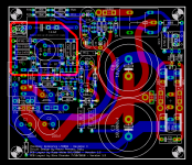
I suppose you're refering to the oblong portion at the top left. That's the outline of the copper-fill area for the signal ground. On the artwork (and the PCB), it will show up as a solid copper area with isolated pads (except a few that are grounded).
It's there (in a slightly different shape) on the Version 1.2 PCB as well.
Thank you - it was very gracious of Mauro to grant permission to use his schematic, and likewise of Russ to post the Eagle files here earlier. It was therefore imperative to acknowledge their contributions. In fact, that is all that Mauro seeks in return for the use of his schematic.
Just one note... Mauro is not from Milan...
If I remember correctly he is from Trento.
If I remember correctly he is from Trento.
Thanks, I'll verify it and make the necessary correction.
From building V 1.2, the following items were noted that you may not have addressed (can't tell for sure without the original Eagle files).
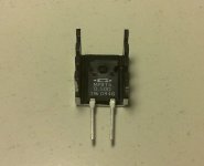
The rear face of the LM3886 should extend past the card edge by about 0.5mm.
C4 and C5 had a 7.5mm lead spacing but it is much easier to buy 10mm lead spaced parts.
C7 was a very tight fit in the new RefC kit. Can't tell if any additional space is allocated in 1.3.
C21 is quite large in the kit and had to be bottom side mounted if it was used at all. The 1.3 layout does not appear to have enough space for a 0.022uF FKP2.
The rear face of the LM3886 should extend past the card edge by about 0.5mm.
On the Version 1.2 PCBs, I found that the LM3886TF was almost flush with the edge , so I left it alone. However, a slight overhang is easy to implement in - I'll do that.
C4 and C5 had a 7.5mm lead spacing but it is much easier to buy 10mm lead spaced parts.
Noted - I'll try to get a dual-spaced outline (i.e. supports both 7.5 and 10mm) by editing some existing outline in the library for these locations.
C7 was a very tight fit in the new RefC kit. Can't tell if any additional space is allocated in 1.3.
Easily done.
C21 is quite large in the kit and had to be bottom side mounted if it was used at all. The 1.3 layout does not appear to have enough space for a 0.022uF FKP2.
I didn't use C21, so I left it at 5 mm. There should be space for 7.5mm, but probably not for 10mm. Let me play around with this a bit - that area is a fairly tight fit already.
C21 FKP2 is 0.2inch pin pitch and 0.22inch wide.
Almost square cross-section then. OK, it can be addressed by moving C9 to the left and then moving C21 a shade to the left.
The 220uF capacitor in the bottom left next to C2 is not labeled.
Noted - the label of C1 was also missing in Version 1.2.
I think the 2x220uf down near the left of the LM3886 I think should be closer to the chip if possible.
People have had trouble with 390R using different brand names as its leads wont fit. Might try a larger hole for it.
Are all the resistors a little bigger? I think if possible all resistors should be larger than the Russ White layout.
Nice job
Uriah
People have had trouble with 390R using different brand names as its leads wont fit. Might try a larger hole for it.
Are all the resistors a little bigger? I think if possible all resistors should be larger than the Russ White layout.
Nice job
Uriah
I think the 2x220uf down near the left of the LM3886 I think should be closer to the chip if possible.
I could move it closer, but I wanted to retain the possibility of using 16mm caps there as a future upgrade, for instance Black Gate STD 220 or 330 uF, 50V or the Muse KZ 220/330 uF, 50V.
I'll see how close to the LM3886 it can be brought - since C17/C18 are not populated in most builds, perhaps I can make C1/C2 flush with C17/C18.
Make the pertinent changes to the location of the LM3886 relative to the board. Mine doesn't fit right at all, it need like 1 more milimeter
Enlarge resistor¡s holes, there are some high end brands that doesn't fit at all.
Don't be afraid at all because of making a bigger board. It worths it and the currently one is already very compact.
Regards,
Regi
Enlarge resistor¡s holes, there are some high end brands that doesn't fit at all.
Don't be afraid at all because of making a bigger board. It worths it and the currently one is already very compact.
Regards,
Regi
OK, here's an updated layout incorporating most of the suggestions. I still have to deal with C21, mitre as well as straighten out some traces, increase some pad diameters and shapes, alter some text sizes and positions, and do some general clean-up before extracting the Gerbers.
Meanwhile, keep the suggestions coming, I'll try to incorporate the high-priority ones before freezing the layout at the middle of this week.
Meanwhile, keep the suggestions coming, I'll try to incorporate the high-priority ones before freezing the layout at the middle of this week.
Attachments
OK, here's an updated layout incorporating most of the suggestions.
...
Meanwhile, keep the suggestions coming, I'll try to incorporate the high-priority ones before freezing the layout at the middle of this week.
Hi LinuxGuru,
one question: why is R7 so big?

Please increase the size of C7, C12, C30, C32 so they can accomodate 7x5 mm caps (like Wima FKP2s...) and update R42 value to 47 R.
I suggest to increase space around R3 to accomodate at least a small TO220 hotsink.
Increase also lead spacing for D2, D3; probably the monolithic bridge can be removed.
I would also remove C17, C18 (unused) to make room for bigger C1, C2
Also take a look at this post of mine, it was no more than a joke but it could be that you find something interesting.
Take care to PCB congestion, the original PCB is already congested. Make a carefull selection of which resitors should be 1/2 watt and which not... (R11 should be 1/2 watt, IMHO)
One final suggestion, make traces more round...like in the original PCB
Attachments
why is R7 so big?
...
I wanted to fit a Kiwame or a KOA-Speer 1W carbon film resistor there - they're quite big.
The other suggestions are noted.
Linuxguru, you certainly do know your way around this amp, and I apologize for my earler comments in the other thread. Many have expressed a desire to improve this board layout, and what you're doing is pretty cool.
What about adding a trace and pads for a CL60 to connect PS ground to safety ground? I know that can be done off board, but including it on the board would satisfy those who want to tie them together. If it's safer and required by law in some places, it might be a good change.
I like the suggestion to remove C17 and C18, perhaps the rectifier, to make room.
Peace,
Tom E
- Home
- Amplifiers
- Chip Amps
- The new "My Ref" Rev C thread