Combi Layout CCS-VAS / BS-VAS
Hello maxlorenz,
in the mean time I prepared a combi layout for CCS-VAS / BS-VAS
acc. to your latest simulation schematics including
cascoded current mirror
cascoded EF
CCS-VAS
don't popate the following parts
C22=100u
C27=220n
R47=1k/3W
R48=1k/3W
R67= opt.
R29=10k
use R68=0R
BS-VAS
don't popoulate the following parts
D43, (D44), D45
T24, T25
(C34), C35
(R78=20)
(R79=100)
(R80=10k)
(R81=1k)
(R82=20R)
(R84=20R)
R86=10k
insert R29=10k
If both variants should be tested
the parts in brackets can be kept in,
the other parts must plugable (contact of a DIP socket)
Remarks
if quality Ecaps are used for PS decoupling I think it's usually not necessary
to bypass them with a film Cap (if required solder underneath Ecap)
check all semiconductors (transistors with bold circle are mounted on heat sink)
Diodes: is 1N4148 OK or better use BAS21 (SMD, mounted to solder layer)
are the following parts necessary
R82, R84, R88, R90 =20R
diode in parallel to C13, C35 =100p (what is the function?)
Drivers + cascode
BD139 / BD140 (MJE340 / MJE350 if Uce>80V required)
I think there is no need to use transistors with bigger case for the cascode
if seize of heat sink is sufficient (T-/L-profile)
check footprint of the following parts
C22, C27
all power resistors
Comments / proposals / improvements are welcome.
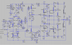
View attachment Amnesis_Combi_Schem.pdf
View attachment Amnesis_Combi_Lay.pdf
Hello maxlorenz,
in the mean time I prepared a combi layout for CCS-VAS / BS-VAS
acc. to your latest simulation schematics including
cascoded current mirror
cascoded EF
CCS-VAS
don't popate the following parts
C22=100u
C27=220n
R47=1k/3W
R48=1k/3W
R67= opt.
R29=10k
use R68=0R
BS-VAS
don't popoulate the following parts
D43, (D44), D45
T24, T25
(C34), C35
(R78=20)
(R79=100)
(R80=10k)
(R81=1k)
(R82=20R)
(R84=20R)
R86=10k
insert R29=10k
If both variants should be tested
the parts in brackets can be kept in,
the other parts must plugable (contact of a DIP socket)
Remarks
if quality Ecaps are used for PS decoupling I think it's usually not necessary
to bypass them with a film Cap (if required solder underneath Ecap)
check all semiconductors (transistors with bold circle are mounted on heat sink)
Diodes: is 1N4148 OK or better use BAS21 (SMD, mounted to solder layer)
are the following parts necessary
R82, R84, R88, R90 =20R
diode in parallel to C13, C35 =100p (what is the function?)
Drivers + cascode
BD139 / BD140 (MJE340 / MJE350 if Uce>80V required)
I think there is no need to use transistors with bigger case for the cascode
if seize of heat sink is sufficient (T-/L-profile)
check footprint of the following parts
C22, C27
all power resistors
Comments / proposals / improvements are welcome.
View attachment Amnesis_Combi_Schem.pdf
View attachment Amnesis_Combi_Lay.pdf
Hello maxlorenz,
in the mean time I prepared a combi layout for CCS-VAS / BS-VAS
acc. to your latest simulation schematics including
If both variants should be tested
the parts in brackets can be kept in,
the other parts must plugable (contact of a DIP socket)
check all semiconductors (transistors with bold circle are mounted on heat sink)
check footprint of the following parts
C22, C27
all power resistors
Comments / proposals / improvements are welcome.
Brilliant work!

diode in parallel to C13, C35 =100p (what is the function?)
Baker clamps, to avoid rail sticking when clipping...the experts recommend them. Optative, in case you wanna party.
Remarks
if quality Ecaps are used for PS decoupling I think it's usually not necessary
to bypass them with a film Cap (if required solder underneath Ecap)
Agreed. I exagerate a lot in size and position, just in case of oscillation but present circuit is stable. I believe some of these are not necessary.
The same for the 20R on decoupling caps: they were inserted to prevent HF noise and oscillation.
R84+R88: they seem to help a little with HF harmonics. Not big thing.
R82+R90: they can be deleted. Not useful.
cascoded current mirror: use R68=0R
I think you can save some space here by using the same holes for either cascode transistors OR 68R resistors...don't you think?
Diodes: is 1N4148 OK or better use BAS21 (SMD, mounted to solder layer)
For the diode string any 1A simple diode. For the rails simple or better Schottky with comparable current handling.
Drivers + cascode
BD139 / BD140 (MJE340 / MJE350 if Uce>80V required)
I think there is no need to use transistors with bigger case for the cascode
if seize of heat sink is sufficient (T-/L-profile)
You're the expert. I am affraid though about the instantaneous handling of power surcharge. Simulations say they should be OK.
I tested what I had here in the form of a 2.5A SMD part and the bias circuit worked OK. They have half the Cob of the 1837/4793 parts though...
Sorry. I will study layout later.
M.
Dear JOSI1 wrote:
The more I look at it, the more I find that I cannot make improvements upon your work of art. I lack the knowledge to critique from a EMI POV.
Some random thoughts...
The gate stoppers for the JFET cascode at the input (R49-R50) are not used on the last build but better be there just in case...
I use 12K or 12K5 (low tempco) as feedback R or its equivalent, 4 parallel or 4 series-parallel, as D. Self demonstrated somewhere its value in reducing distortion. My last build uses 4*51K hi quality.
What is better for the Vbe multiplier transistor (T9) in terms of EMI, polution or contamination as it passes near the output: as you have it now or with the leads braided and aerial?
Or, is there a way to have the Vbe multiplier nearer?
OK for now.
Cheers,
M.
Comments / proposals / improvements are welcome.
The more I look at it, the more I find that I cannot make improvements upon your work of art. I lack the knowledge to critique from a EMI POV.
Some random thoughts...
The gate stoppers for the JFET cascode at the input (R49-R50) are not used on the last build but better be there just in case...
I use 12K or 12K5 (low tempco) as feedback R or its equivalent, 4 parallel or 4 series-parallel, as D. Self demonstrated somewhere its value in reducing distortion. My last build uses 4*51K hi quality.
What is better for the Vbe multiplier transistor (T9) in terms of EMI, polution or contamination as it passes near the output: as you have it now or with the leads braided and aerial?
Or, is there a way to have the Vbe multiplier nearer?
OK for now.
Cheers,
M.
I was premature in my comments, as sometimes happens...
After several CDs, I realized that something was odd: there was a hardness unusual; there was a predominance of HF over other frequencies. After inspection, I discovered that I had let in place the 220n capacitors from the previous biasing circuit (LED+R) and simulations showed weird things on the output when used on the present biasing (zener +R) though the scope did not show any anomaly...I removed the offenders, but, halas, one of the channels started that dreadful oscillation of the negative peaks!
With my useful sang froid I reinstalled only the caps for the negative side apparently this circuit hates symmetry because it worked. Not only oscillations disappeared but the sound regained its "morbidezza" as Italian say. So, we must expect the unexpected in the real world.
I should experiment with different combinations of decoupling, from node to ground and from node the rail perhaps.
Since behavior on the experimental board cannot be completelly asured, I think you should contemplate the addition of space for tinny film capacitors from node to ground at least on the negative side...
Cheers,
M.
Edit: simulations show that 220n is too much because gross distortion appears at -16V. 100n will give you +/-25V swing and 22n to 10n will give you clean +/-35V output swing.
After several CDs, I realized that something was odd: there was a hardness unusual; there was a predominance of HF over other frequencies. After inspection, I discovered that I had let in place the 220n capacitors from the previous biasing circuit (LED+R) and simulations showed weird things on the output when used on the present biasing (zener +R) though the scope did not show any anomaly...I removed the offenders, but, halas, one of the channels started that dreadful oscillation of the negative peaks!
With my useful sang froid
I reinstalled only the caps for the negative side apparently this circuit hates symmetry because it worked. Not only oscillations disappeared but the sound regained its "morbidezza" as Italian say. So, we must expect the unexpected in the real world.I should experiment with different combinations of decoupling, from node to ground and from node the rail perhaps.
Since behavior on the experimental board cannot be completelly asured, I think you should contemplate the addition of space for tinny film capacitors from node to ground at least on the negative side...
Cheers,
M.
Edit: simulations show that 220n is too much because gross distortion appears at -16V. 100n will give you +/-25V swing and 22n to 10n will give you clean +/-35V output swing.
Attachments
Last edited:
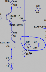
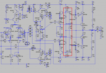
Hi Max,
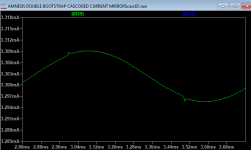
are the R+C networks you refer to R27 + C9 shown in first image?
I suggest that as drawn this is effectively appears a a capacitive load on the output of the amplifier. I don't think this was your intention.
I have been thinking for a while that capacitors across the cascode zeners might help as shown in second image. This arrangement should help maintain bias current in the cascode transistors as the output approaches rail. I know this could cause the voltages Collector / Base junction to be reversed at extreme output swing so the resistor value should not be zero, and the capacitors should not be large values.
As always, these are just suggestions and it's what sounds best that counts.
Regards,
Symon
Attachments
Dear Symon,
Exactly my thoughts.
That were very late night quick simulations to avoid gross distortion.
In my case, oscillations were higher than 10MHz so I can use very low capacitance here and I can test both sides and even the output cacodes, just in case.
With 2K and 220pF the corner frequency would be 361.89 KHz. I think that would not overload the transistors. Anyway, the R=0 shows that I was using a small R for testing A 20-100R should not harm.
I really prefer to bypass to ground...or better, not to bypass to output. I'll simulate later when I have time...I will try also from node to node, an C-R-C.
Anybody has further thoughts on this topic?
The eventual oscillation will depend on parasitics and grounding scheme on each particular case.
BTW, I also installed the cap on the "good" board, just for the sake of tranquility but, even though the sounds is good and the amp seems stable, the LEDs for the VAS cascode dim a little with the music
Listening to some Mombasa from the 70's ...and now Sam Cooke.
Thanks for the support.
M.
Exactly my thoughts.
That were very late night quick simulations to avoid gross distortion.
In my case, oscillations were higher than 10MHz so I can use very low capacitance here and I can test both sides and even the output cacodes, just in case.
With 2K and 220pF the corner frequency would be 361.89 KHz. I think that would not overload the transistors. Anyway, the R=0 shows that I was using a small R for testing
A 20-100R should not harm.I really prefer to bypass to ground...or better, not to bypass to output. I'll simulate later when I have time...I will try also from node to node, an C-R-C.
Anybody has further thoughts on this topic?
The eventual oscillation will depend on parasitics and grounding scheme on each particular case.
BTW, I also installed the cap on the "good" board, just for the sake of tranquility but, even though the sounds is good and the amp seems stable, the LEDs for the VAS cascode dim a little with the music
Listening to some Mombasa from the 70's
...and now Sam Cooke.Thanks for the support.
M.
Last edited:
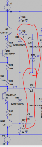
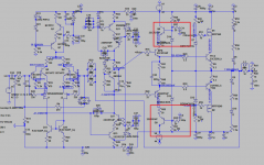
Hi Max,
I think you need to consider that decoupling should be to the reference point for each circuit element. Looking at your circuit, the current sources are decoupled to ground. But they are referenced to the positive rail, as currently connected the capacitors inject any rail noise into the current sources.
The second drawing shows connected the decoupling to make the current source voltage reference more stable since this is referenced to rail not ground. Also note that I believe C35 should be removed as id defeats C8 which is stabalising the diode reference voltage. So keep C8 and delete C35, unless you like the sound it produces.
Regards,
Symon
I really prefer to bypass to ground...or better, not to bypass to output. I'll simulate later when I have time...I will try also from node to node, an C-R-C.
Anybody has further thoughts on this topic?
I think you need to consider that decoupling should be to the reference point for each circuit element. Looking at your circuit, the current sources are decoupled to ground. But they are referenced to the positive rail, as currently connected the capacitors inject any rail noise into the current sources.
The second drawing shows connected the decoupling to make the current source voltage reference more stable since this is referenced to rail not ground. Also note that I believe C35 should be removed as id defeats C8 which is stabalising the diode reference voltage. So keep C8 and delete C35, unless you like the sound it produces.
Regards,
Symon
Attachments
Hi Max,
I think you need to consider that decoupling should be to the reference point for each circuit element. Looking at your circuit, the current sources are decoupled to ground. But they are referenced to the positive rail, as currently connected the capacitors inject any rail noise into the current sources.
The second drawing shows connected the decoupling to make the current source voltage reference more stable since this is referenced to rail not ground. Also note that I believe C35 should be removed as id defeats C8 which is stabalising the diode reference voltage. So keep C8 and delete C35, unless you like the sound it produces.
Regards,
Symon
You beat me to the punch. So, your advice is taking all those decoupling caps better to the rails? And keep them small, right.
Well I did some simulations to make sure the circuit does not clip early.
The following decoupling is stable on paper and produces 0.002% THD pre-clipping. It also works for the cascode output. I checked it.
The problem is that, when oscillations occurs, unnexpected things (at least by me) happen: once I decoupled a cascode node (1uF) to the rail and the transistor exploded instantly
So my plan was make the simplest decoupling connection, with arguably the least energy flux, that makes the circuit stable...Thanks very much for your sound advice. I suspected my decoupling was excessive/wrong.
I believe I will have some time to experiment today.
Best wishes,
M.
Attachments
maxlorenz;5511324: once I decoupled a cascode node (1uF) to the rail and the transistor exploded instantly[/QUOTE said:Hi Max,
I think you miss understood my last post 187, I was refering to the decoupling capacitors on hte input and Vas stage current sources.
The output stage cascodes should maintain a constant voltage across the output devices. so I would not connect the decoupling capacitors to ground or rail.
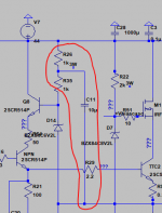
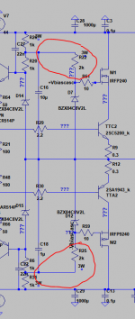
A better idea is to split the Zener serise resistors in half and add a boot strap capacitor. See attached, this will help keep the current through the zener stable at extreme output swing.
Regards,
Symon
Attachments
Hi Max,
I think you miss understood my last post 187, I was refering to the decoupling capacitors on hte input and Vas stage current sources.
Yes, I got that. I started to play with low value caps (47n to 220n) in places you recommended and at some point I got 0.0007% THD near clipping, but then I kept on and lost it...The only big cap whose elimination led to worse THD was C35.
Carlinhos uses bootstrap also for his input CCS. We can add independent bootstrap everywhere where CCS is needed.
The output stage cascodes should maintain a constant voltage across the output devices. so I would not connect the decoupling capacitors to ground or rail.
A better idea is to split the Zener serise resistors in half and add a boot strap capacitor. See attached, this will help keep the current through the zener stable at extreme output swing.
Regards,
Symon
Brilliant! I suspected bootstrap would be useful somewhere but my own experiment/simulation (with cascoded-CFP output) went very bad. Lucky that you know your stuff. It could even work on output...
It's combining a voltage source with a CCS, with the added benefit of reducing the stress for the resistors by half. Could use 1W or 2W resistors.
Bootstrap gives a certain easyness to the music.
I would have to work underneath the board, though. Not enough space. I still have some good 10u film caps.
Phylosophically, I am concerned about the caps not being Low Thermal Memory approved...
Cheers,
M.
Attachments
Dear Symon wrote:
Quick update.
Yesterday I swapped the existing C9= 220nF for a 22nF. It does not oscillate, nor does its sibling without any cap in that position, listening some funky music from the 70's at the risk of disturbing the neighbors
With 560pF it still oscillated like mad on negative peaks. I was lazy and did not try intermediate values.
Could it still be capacitive loading if the zeners protect the outputs?
I think I remember stability margins were unchanged...I got to check it.
Anyway, sounding good.
As is, the Amnesis will not disappoint. It is easy to make a PCB the old fashion.
Dear JOSI1: I will keep studying the bypassing to make a definitive version of it.
Since I have to repair the bootstrapped VAS amp, I decided to use there the series resistors to install the optional bootstrapped version of the zener biasing circuit later, when all is OK. There I have more room and using some good 47u electros I will still have more space.
Cheers,
M.
Hi Max,
are the R+C networks you refer to R27 + C9 shown in first image?
I suggest that as drawn this is effectively appears a a capacitive load on the output of the amplifier. I don't think this was your intention.
Quick update.
Yesterday I swapped the existing C9= 220nF for a 22nF. It does not oscillate, nor does its sibling without any cap in that position, listening some funky music from the 70's at the risk of disturbing the neighbors
With 560pF it still oscillated like mad on negative peaks. I was lazy and did not try intermediate values.
Could it still be capacitive loading if the zeners protect the outputs?
I think I remember stability margins were unchanged...I got to check it.
Anyway, sounding good.
As is, the Amnesis will not disappoint. It is easy to make a PCB the old fashion.
Dear JOSI1: I will keep studying the bypassing to make a definitive version of it.
Since I have to repair the bootstrapped VAS amp, I decided to use there the series resistors to install the optional bootstrapped version of the zener biasing circuit later, when all is OK. There I have more room and using some good 47u electros I will still have more space.
Cheers,
M.
Listening tests going on, with different digital sources. Chamber music.
I will try to evaluate increased biasing also.
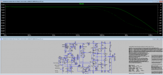
Bode plot unaltered with good margins.
No time to play until perhaps Sunday but here is the plan and a revised bypassing option.
Cheers,
M.
I will try to evaluate increased biasing also.
Could it still be capacitive loading if the zeners protect the outputs?
I think I remember stability margins were unchanged...I got to check it.
Bode plot unaltered with good margins.
Since I have to repair the bootstrapped VAS amp, I decided to use there the series resistors to install the optional bootstrapped version of the zener biasing circuit later, when all is OK. There I have more room and using some good 47u electros I will still have more space.
No time to play until perhaps Sunday
but here is the plan and a revised bypassing option.Cheers,
M.
Attachments
Last edited:
Hi Max,
the new circuit looks interesting, I'm interested to hear what it sounds like.
I did a few experiments in the simulator mainly as to why removing C35 increased distortion, and have a few observations:
The current running throug the input constant current voltage references is rather high, in fact for R8 it's 6mA, and in R32 its about 2.5mA. given hte gain of the transistors you probably need less than 1mA. THis wil reduce the load on the filtered supply. Which I notice in this simulation has it's own voltage source V1? I assume V1 isn't in the real circuit?
Increasing the values of C4 and C26 to say 1000u looks like it will provide useful real world improvement.
Regards,
Symon
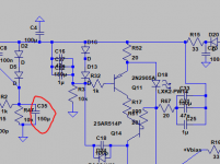
Hi Max,
I checked the input stage current and in hte simulation it shows signs of cross over distortion. This shows up as spikes on the current through he emitter resistors. see attached.
The simulated output stage bias current is very low at 12mA, I altered the value of R123 from 1.2K to 1.33K which sets a bias current of around 65mA in the output stage. This helps a lot an reduces distortion values at high and low signal levels.
Out of curiosity what output stage bias current do you set on the real amplifiers? And I assume in the real amplifier R24 is a preset?
Regards,
Symon
Attachments
Hi Max,
the new circuit looks interesting, I'm interested to hear what it sounds like.
I did a few experiments in the simulator mainly as to why removing C35 increased distortion, and have a few observations:
The current running throug the input constant current voltage references is rather high, in fact for R8 it's 6mA, and in R32 its about 2.5mA. given hte gain of the transistors you probably need less than 1mA. THis wil reduce the load on the filtered supply. Which I notice in this simulation has it's own voltage source V1? I assume V1 isn't in the real circuit?
Increasing the values of C4 and C26 to say 1000u looks like it will provide useful real world improvement.
Regards,
Symon
Dear Sir,
Once again you are completelly right.
I revised again (R8-R27-R32; ) as recommended. It works as you said and not only THD but also "noise floor" (at least I believe) went down significantly.
The extra V1 (an error) was a remain of an "external" PS for the inputs...which will be a nice experiment, BTW.
Given the multitude of combinations for input CFP resistors (R5-R10/R33-R34) I chose another one that looks interesting: 1K5 + 100R. Worth a try...
Playing with the inter-transistor R63 also varies the THD profile, without altering (within reasonable values of R63) the current at the input section. No idea if this is important or not. Someday I will remember to experiment with that one...endless permutations...
I checked the input stage current and in hte simulation it shows signs of cross over distortion. This shows up as spikes on the current through he emitter resistors. see attached.
The simulated output stage bias current is very low at 12mA, I altered the value of R123 from 1.2K to 1.33K which sets a bias current of around 65mA in the output stage. This helps a lot an reduces distortion values at high and low signal levels.
Out of curiosity what output stage bias current do you set on the real amplifiers? And I assume in the real amplifier R24 is a preset?
R24 is in reality (check .png whyte schematics) a 1K pot in series with a 470R: that pot (and not R23) is used to play with current bias.
You know I am coward (reckless coward in fact) so I run the output of the amp, in this experimental phase, fairly low, perhaps under 10mA.
As I said before, I am now increasing it slowly and listening, now that I know it is stable.
Simulations show that under 100mA it should be still stable. I also fitted the optional (in case of oscillation) 22nF caps (C22-C27) and nothing obviously wrong occured...
I always forgot to mention something about the LEDs of the last build:
1) for the cascoded CCS of the input (D11...etc) I am using in reality 3 blue LEDs which give around 10V lower than the rail. They look nice, but in the future, with the next 33K to ground R8, they will look less impressive.
This voltage is not that critical as long as it gives room for the VCE of the main transistor: I wanted to know how the cascoded-CCS would work in case I decide to increase the PS to more than 50V.2) for the cascoded VAS I am using 2 yellow LEDs, which give me around 4V from the rail or around 3.6V VCE for the VAS transistor, last time I checked.
Attachments
Last edited:
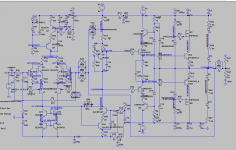
Hi Max,
this version looks a lot better, but how does it sound?
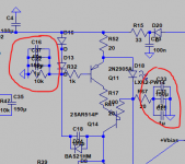
A Suggestion to improve output swing is to connect the MOSFET resistors R22 and R25 to the Driver bootstrap as shown in attached. This will keep the MOSFETs conducting as the output approaches rail voltages, and this reduces clipping at high outputs.
The capacitors C22 and C27 are new, and although simulation sggests they don't affect distortion, I'm not sure why they are there to promote stability?
Unfortunately I believe they will inject rail noise into the driver cascode, so if they are required for stability connect them to ground rather than rail. Although my preference would be to connect them to the output so they are not exposed to large voltage swings. But this is something for experimentation.
Regards,
Symon
this version looks a lot better, but how does it sound?
A Suggestion to improve output swing is to connect the MOSFET resistors R22 and R25 to the Driver bootstrap as shown in attached. This will keep the MOSFETs conducting as the output approaches rail voltages, and this reduces clipping at high outputs.
The capacitors C22 and C27 are new, and although simulation sggests they don't affect distortion, I'm not sure why they are there to promote stability?
Unfortunately I believe they will inject rail noise into the driver cascode, so if they are required for stability connect them to ground rather than rail. Although my preference would be to connect them to the output so they are not exposed to large voltage swings. But this is something for experimentation.
Regards,
Symon
Attachments
Hi Max,
regarding output stage bias, the current value is critical to obtaining low distortion.
The problem is maintaining the correct bias value as the devices warm up, fortunately because the drivers and output devices are cascoded they are not exposed to large voltage swings of conventional EF outputs. So we expect the heating effect to be reduced in the critical devices, and perhaps make the bias more stable.
Because of design the bulk of the power is disipated in the cascode devices M1, M2, Q8 and Q9, perhaps these should be on a separate heatsink.
Then have a smaller heatsink for the drivers, output devices and have the temperature sensor on this. The smaller heatsink will make the sensor quicker to respond to temperature changes.
Long ago I built an amplifer that kept suffering thermal run away, eventually I added a simple current limiter to output stage, which limited the current to a safe level. This prevents the then expensive output devices from being destroyed but set high enough that the fuses blow.
I suggest adding this feature if only for developent.
Regards,
Symon
Hi Symon,
Only simulations for now. Not much time to heat the iron lately.
This option would be available when I repair the bootstrapped amp. Improvements for the input biasing bypass will be done as time allows...
I have shown before a circuit that included also an independent bootstrap for the MOSFETs but, due that simulation shows that the gate only eats up fractions of a FemtoAmp, I think it would be excessive, even for me, hehe. Add to that that I will probably never use the amp nowhere near clipping. Feel free to try it later, though, if you want to crank-up the volume.
Edit: I forgot to evaluate what happens at clipping on that circuit...
Yes, you are right again. My mistake due to precipitation. Those capacitors are optional, only in case there is oscillation present, which is usually contaminating the negative side and only at musical peaks: only one should be connected, on the offending side, and to ground (not rail), given my recent experience with one of the boards (the other is free from oscillation) of the CCS-loaded VAS amp. I was just testing if and when I make the bootstrap for the drivers, I would be still able to use this trick...
Update on output current bias.
I made a tactic mistake when I built the CCS-loaded VAS amp: for convenience, I connected the 0R33 emitter output resistors on the under side of the board so it is not easy to measure. It saved me lots of space though...
Now I am listening "Violins of Cremona" with Salvatore Accardo, with 45mA per side at the outputs (650mV from base to ground for the MJE15024/25 cans) and it obviously sounds better than sub-biased. Reduced graininess, more micro-detail, more nuances, more solidity to the images. Dynamics also are more violent. Easier to spot timbral differences between violins.
Other thoughts.
In order to improve input-VAS matching, we can increase input pair current to 4 or 5mA per side and use something better as VAS transistor. I have here some MPSA18 that I imagine will be good on that position.
Thanks again for your invaluable input and support.
Yours truly,
M.
this version looks a lot better, but how does it sound?
Only simulations for now. Not much time to heat the iron lately.
This option would be available when I repair the bootstrapped amp. Improvements for the input biasing bypass will be done as time allows...
A Suggestion to improve output swing is to connect the MOSFET resistors R22 and R25 to the Driver bootstrap as shown in attached. This will keep the MOSFETs conducting as the output approaches rail voltages, and this reduces clipping at high outputs.
I have shown before a circuit that included also an independent bootstrap for the MOSFETs but, due that simulation shows that the gate only eats up fractions of a FemtoAmp, I think it would be excessive, even for me, hehe. Add to that that I will probably never use the amp nowhere near clipping. Feel free to try it later, though, if you want to crank-up the volume.
Edit: I forgot to evaluate what happens at clipping on that circuit...
The capacitors C22 and C27 are new, and although simulation sggests they don't affect distortion, I'm not sure why they are there to promote stability?
Unfortunately I believe they will inject rail noise into the driver cascode, so if they are required for stability connect them to ground rather than rail. Although my preference would be to connect them to the output so they are not exposed to large voltage swings. But this is something for experimentation.
Yes, you are right again. My mistake due to precipitation. Those capacitors are optional, only in case there is oscillation present, which is usually contaminating the negative side and only at musical peaks: only one should be connected, on the offending side, and to ground (not rail), given my recent experience with one of the boards (the other is free from oscillation) of the CCS-loaded VAS amp. I was just testing if and when I make the bootstrap for the drivers, I would be still able to use this trick...
Update on output current bias.
I made a tactic mistake when I built the CCS-loaded VAS amp: for convenience, I connected the 0R33 emitter output resistors on the under side of the board so it is not easy to measure.
It saved me lots of space though...Now I am listening "Violins of Cremona" with Salvatore Accardo, with 45mA per side at the outputs (650mV from base to ground for the MJE15024/25 cans) and it obviously sounds better than sub-biased. Reduced graininess, more micro-detail, more nuances, more solidity to the images. Dynamics also are more violent. Easier to spot timbral differences between violins.
Other thoughts.
In order to improve input-VAS matching, we can increase input pair current to 4 or 5mA per side and use something better as VAS transistor. I have here some MPSA18 that I imagine will be good on that position.
Thanks again for your invaluable input and support.
Yours truly,
M.
Hi Max,
regarding output stage bias, the current value is critical to obtaining low distortion.
The problem is maintaining the correct bias value as the devices warm up, fortunately because the drivers and output devices are cascoded they are not exposed to large voltage swings of conventional EF outputs. So we expect the heating effect to be reduced in the critical devices, and perhaps make the bias more stable.
Because of design the bulk of the power is disipated in the cascode devices M1, M2, Q8 and Q9, perhaps these should be on a separate heatsink.
Then have a smaller heatsink for the drivers, output devices and have the temperature sensor on this. The smaller heatsink will make the sensor quicker to respond to temperature changes.
Long ago I built an amplifer that kept suffering thermal run away, eventually I added a simple current limiter to output stage, which limited the current to a safe level. This prevents the then expensive output devices from being destroyed but set high enough that the fuses blow.
I suggest adding this feature if only for developent.
Regards,
Symon
Oh. Cross posting. Read what I updated regarding outputs.
The Hagerman Vbe multiplier is very stable. See the short article if you didn't yet. It also contains the information to calculate R36 (= 4 Ohm in my schematic) given chosen Vbe transistor.
The main heatsink for the cascoded output is cold with 45mA.
The cascoded drivers and cascoded VAS and CCS have their own little heatsink (HS): only the VAS is slightly warm to the touch, and so does corresponding CCS. Drivers' HS is cold.
So, at this point I believe further protection circuitry is not needed.
I am not concerned by thermal runaway but by instantaneous thermal challenge for the internal junctions, from power peaks or heavy oscillation, before the transistors can transfer the heat...
Cheers,
M.
Attachments
Dear Symon, guys,
Your bootstrap idea for the CCS of the cascode's Vsource is getting more interesting and succulent.
I checked with independent bootstrap (lets call it "triple bootstrap") for drivers and output and simulations predict we gain at least 3V (at least 38V swing from a 44V PS) of headroom and clipping starts "softly", though I am not expert in this topic.
(This is with the cascoded VAS- not the cascoded-cascoded-VAS: I forgot to test this one and probably that will limit swing by itself)
I hope this increased headroom is also accompanied by increase in perception of dynamics. Your version of a shared bootstrap (lets call it "double bootstrap") is more elegant and has fewer parts. It has slightly more THD, though. We'll see if this translates to any obvious change in sonics...
Have you all a good musical weekend,
M.
- Home
- Amplifiers
- Solid State
- The AMNESIS amp: a good amplifier, like a gentleman, has no memory.