Having said that, I conclude your priority is to make a good, interesting build project rather than a high performance pre-amp. Eg: you have chosen to copy a NAD phono stage. Which is perfectly fine.")
What is interesting was the quest to duplicate the Niam sound. I am afraid that whatever you hang in-front of the amplifier is going to determine much of its character and the main amp contribution will be masked by that of the pre-amp.
I believe it will follow the effect of contributing noise in a multistage circuit. The first stage will contribute most of the character, the second stage will amplify it and add its own character, the third stage would amplify the previous stages and add its own an so on.
In my opinion you will end up with a more powerful NAD3020, not what you set out to do.
Member
Joined 2009
Paid Member
Well there's some powerful questions in there Nico!
I believe that unless I clone a NAC pre-amp there's little hope of getting anything like the NAIM sound. I simulated the NAC gain stage - with it's 24V single supply - and found a clear distortion profile that is dominant 2nd order harmonic due to it's input stage etc. By the time I convert it to dual rail +/-30V the distortion is greatly reduced. Then if I dial back the large gain it carries to something more 'modern' I end up with very low distortion indeed - nothing of the character of it's implementation in the NAC. So I'm realizing that I can either clone a NAC or my goals have to be different. There may be merit in having the ability to dial in some 2nd harmonic distortion though - I believe it was a key element in the NAC gain stage and it's universally acknowledged to be one of the features of some pre-amps and power-amps that people like with certain kinds (mostly simple) of music.
I looked on a couple of other forums, folk with modern CD sources were modifying their NACs to pull the gain down, or else their volume controls were hardly off the starting line. One chap found the gain stage became unstable at low gain so there was a limit to what he could accomplish but with lower gain he said the sound was much better, cleaner. A few months later he made further changes and took the gain stage out of the signal path, sending the signal through a buffer instead - said it cleaned up the sound no-end and he liked it even more. So there we have it - a full clone for the NAIM sound or this project will be honest to a different goal.
I will eventually build (rpi) or buy a digital source and likely it'll be the main source of music. Not sure when that will happen as it gets hard to find time - I haven't listened to music for over a year now so no rush. Anyhow, this means that my priority is not necessarily the sound of the phono amp. I have several DIY power amps. My NAIM clone (haven't finished that one yet - needs to be tweaked) is only one. One of the goals of the preamp was to have a clean sound so that I can 'hear' my power amps.
Realizing that I have several power amps, I wonder if there's merit to include an active cross-over board so that I can try bi-amping one day.
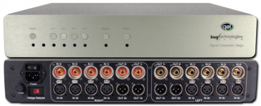
Here are a couple photos of the BSG Technologies QOL box from the review at 6moons.com. They used a whole bunch of relays (black rectangular boxes) to implement the input and output selectors. Power supply at right, near the toroidal transformer, is fairly elaborate. Signal handling at left, is just opamps and resistors. The (grey) film capacitors are used for supply bypassing, which is why they are abutted to the top and bottom of the opamp DIP8 packages. Pin8 at top is VCC+, Pin4 at bottom is VEE-. Yellow capacitors are few-pF bypass across the feedback resistor. Opamps sport the Burr-Brown logo.
Here is a guy who compared a QOL box side-by-side with a DSP implementation of standard Blumlein Mid+Side width enhancement and found them to be identical. What's inside the box they're selling, is their first "golden ratio" patent. Not their second patent with all the woo-woo layering.
_
Here is a guy who compared a QOL box side-by-side with a DSP implementation of standard Blumlein Mid+Side width enhancement and found them to be identical. What's inside the box they're selling, is their first "golden ratio" patent. Not their second patent with all the woo-woo layering.
_
Attachments
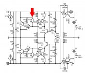
Which one is the same-sex version, the top or bottom schematic in post 506?
What controls the output voltage, the Zeners or something else?
Thanks.
Guess my questions weren't important enough to answer.
Member
Joined 2009
Paid Member
You'll have to tell that to On-Semi...Odd that no-one noticed this.
Attachments
When you correct the hookup error of R103 and its fraternal twin sister, output impedance will fall appreciably. In my simulation Zout was reduced by a factor of two. Odd that no-one noticed this.
_
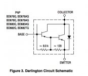
The Darlington arrangement seemed to have been to be based on the circuit representation of the likes of TIP120 and TIP125 - https://www.onsemi.com/pub/Collateral/TIP120-D.PDF a detail of which got lost in the translation.
Soldering SMD 8k resistors in the correct position on the underside is one possible fix using the existing board layout.
Member
Joined 2009
Paid Member
Which one is the same-sex version, the top or bottom schematic in post 506?
What controls the output voltage, the Zeners or something else?
Thanks.
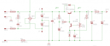
In #506 the same-sex version is the bottom one of the two schematics. In the Zout plot the outputs are labelled "V++" and "V--".
The output voltage is set by the Zener diodes.
These diodes establish a fixed voltage drop across themselves in normal use. They're not ideal as reference voltage providers but it's fine for this application.
The regulator input transistors (not the CCS devices) in #506 are labelled Q22, Q37 for the top and Q2 and Q4 for the bottom. They are the 'error' amplifier, comparing the voltage at their emitters (signal ground) and base (held at 30V away from the rail). In my LTSpice simulation I used two 15V zener diodes, whereas in my pcb layout I use only one 30V zener. Any difference in voltage between base-emitter results in a current flow through their collectors.
The regulator input transistors have current mirrors on their collectors to provide a very high impedance. Even a small error signal current through the collectors will result in large voltage swings because of this high impedance. This ensures they operate at highest possible gain. The voltage signal drives the shunt element, shown in my LTspice simulation as a pair of transistors and resistors but in reality is a single Darlington transistor in a TO-126 package. I was trying to simulate what I saw in the On-Semi datasheet - I have no intention of adding these resistors but assumed they were present inside the package. If they are not present inside the package then I won't have having any such resistors in the circuit.
You'll have to tell that to On-Semi...
You should check the connections more closely. The 8k resistor should connect between Q64 base and emitter.
Last edited:
Member
Joined 2009
Paid Member
Oh I see what you mean ! ha, well, call it schematic dyslexia, or schelexia. New word. Anyhow, for the real-world pcb these resistors are not there. And re-running the simulations after fixing that shows the Zout is suitably tiny - we'll not be finding Zout a parameter to worry about. Actually, there's another error in that simulation (can you see it?).
Attachments
Last edited:
Member
Joined 2009
Paid Member
Member
Joined 2009
Paid Member
Oh I see what you mean ! ha, well, call it schematic dyslexia, or schelexia. New word. Anyhow, for the real-world pcb these resistors are not there. And re-running the simulations after fixing that shows the Zout is suitably tiny - we'll not be finding Zout a parameter to worry about. Actually, there's another error in that simulation (can you see it?).
I see you have since fixed this - the missing 10k resistor in the lower half of your circuit.
Last edited:
OK. But there's an easy way to lower it yet another ~3X without modifying the PCB layout. Just changing SMD component values. And with no impact upon stability / phase margin.... - we'll not be finding Zout a parameter to worry about.
Warning: science required.
Hi guys, I haven't been following this thread closely at all so apologies if already asked and answered...
Do you really need to tightly regulate both rails, or can you arrange your discrete stages so that you only need one regulator?
For example, the simple 2T discrete buffer and shunt feedback stages I've played with have truly awful PSR on only one rail, so I use a +ve regulator and a simple RC filter for the -ve.
Attachments
In #506 the same-sex version is the bottom one of the two schematics. In the Zout plot the outputs are labelled "V++" and "V--".
The output voltage is set by the Zener diodes.
These diodes establish a fixed voltage drop across themselves in normal use. They're not ideal as reference voltage providers but it's fine for this application.
The regulator input transistors (not the CCS devices) in #506 are labelled Q22, Q37 for the top and Q2 and Q4 for the bottom. They are the 'error' amplifier, comparing the voltage at their emitters (signal ground) and base (held at 30V away from the rail). In my LTSpice simulation I used two 15V zener diodes, whereas in my pcb layout I use only one 30V zener. Any difference in voltage between base-emitter results in a current flow through their collectors.
The regulator input transistors have current mirrors on their collectors to provide a very high impedance. Even a small error signal current through the collectors will result in large voltage swings because of this high impedance. This ensures they operate at highest possible gain. The voltage signal drives the shunt element, shown in my LTspice simulation as a pair of transistors and resistors but in reality is a single Darlington transistor in a TO-126 package. I was trying to simulate what I saw in the On-Semi datasheet - I have no intention of adding these resistors but assumed they were present inside the package. If they are not present inside the package then I won't have having any such resistors in the circuit.
Thank you for the detailed explanation!
Member
Joined 2009
Paid Member
What simulation could I run to check if my RIAA has sufficient slew rate (to drive the feedback network) ?
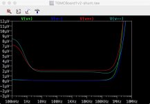
If I hand a current source off the output of the emitter follower, where the feedback is taken from, I can simulate the Zout of this point (with 470uF fdbk shunt cap). It looks as attached (vertical scale is ohms). If I understand correctly, I would be worried about slew rate if this Zout is comparable or higher than the fdbk shunt resistor at 56ohm.
If I hand a current source off the output of the emitter follower, where the feedback is taken from, I can simulate the Zout of this point (with 470uF fdbk shunt cap). It looks as attached (vertical scale is ohms). If I understand correctly, I would be worried about slew rate if this Zout is comparable or higher than the fdbk shunt resistor at 56ohm.
Attachments
Member
Joined 2009
Paid Member
Interesting comment on the tone control: http://www.diyaudio.com/forums/solid-state/196384-anybody-have-formal-loudness-circuit.html
I'd recommend you use Bob Cordell's slew rate criterion from section 6.1 of his book. Adjusting for RIAA it would be something like this:
Other people just feed a square wave into the inverse-RIAA network and measure the slope of the rising edge and falling edge of the trapezoidal wave at the amplifier output. deltaVolts/deltaSeconds = slew rate. But, eeew.
1. Connect an inverse-RIAA network between the simulation signal generator and the simulation preamp.
2. Set the simulation signal generator to 1 kHz and adjust its amplitude until the preamp output is maximum (e.g. 200 mV before clipping)
3. Now with the same amplitude, set the simulation signal generator frequency to 50 kHz per Bob Cordell
4. Look for slew rate limiting. It will manifest itself in the VBE of the output emitter follower Q503. If Q503's VBE falls ~ 75 millivolts below its value at 1kHz, you got slew rate limiting. Or, have the simulator measure Total Harmonic Distortion; if it's gigantically bigger at 50 kHz than at 1 kHz, you got slew rate limiting.
Other people just feed a square wave into the inverse-RIAA network and measure the slope of the rising edge and falling edge of the trapezoidal wave at the amplifier output. deltaVolts/deltaSeconds = slew rate. But, eeew.
Attachments
Member
Joined 2009
Paid Member
Thanks - I'll give this a proper look.I'd recommend you use Bob Cordell's slew rate criterion ...
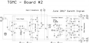
In meantime, I started to rough-out Board#2, the tone control with output driver. I am thinking about the possibility of the output buffer being dc-stable wrt to temperature so that I can build it without coupling cap?
Missing is an output 'mute' - haven't decided on best option, probably a relay with delayed-on.
Attachments
- Status
- This old topic is closed. If you want to reopen this topic, contact a moderator using the "Report Post" button.
- Home
- Source & Line
- Analog Line Level
- TGMC - a modular control pre-amplifier