Gareth,
I suspect the offset tetchiness is caused by the high transconductance of the complementary VAS; if you replace them with mosfet variants such as ZVP2210G and ZVN2210G the tetchiness should disappear entirely, and moreover the loop gain, already high, will drop by about 20dB, giving it a sound quality more like Andrej's original lateral fet circuit. Loop gain affects sound quality, as you know.
Cheers,
Hugh
Member
Joined 2009
Paid Member
Hi Hugh,
yes, those SOT-363 packages look rather small. I got one from the stores at work to look at (it's not a transistor array but the package is the same). It's really tiny ! I'm actually more worried about being able to make pcb traces that small at home (toner transfer) than I am with being able to solder them. I think I had better benefit from your experience here and avoid backing myself into a corner on these small things quite yet.
The FET VAS is an interesting idea. Trouble is, this is an "all BJT" design so this is one option I have already cut myself off from. I am wondering anyhow, if I can't get the same benefit by increasing the emitter degeneration on a BJT VAS ? In theory I can degenerate down the transconductance to the same level as a FET and at the same time have excellent linearity because of the local feedback it provides.
High loop gain is addictive though, especially when you look at the Spice results heck, maybe I should toy with the idea of cascoding the VAS for a further bump. I need therapy !
yes, those SOT-363 packages look rather small. I got one from the stores at work to look at (it's not a transistor array but the package is the same). It's really tiny ! I'm actually more worried about being able to make pcb traces that small at home (toner transfer) than I am with being able to solder them. I think I had better benefit from your experience here and avoid backing myself into a corner on these small things quite yet.
The FET VAS is an interesting idea. Trouble is, this is an "all BJT" design so this is one option I have already cut myself off from. I am wondering anyhow, if I can't get the same benefit by increasing the emitter degeneration on a BJT VAS ? In theory I can degenerate down the transconductance to the same level as a FET and at the same time have excellent linearity because of the local feedback it provides.
High loop gain is addictive though, especially when you look at the Spice results
heck, maybe I should toy with the idea of cascoding the VAS for a further bump. I need therapy !is about all you can say, unless the full specification tells you more about wafer and matching and pairs, etc.they will track temperature changes together.
But, the thermal contribution from the leads and PCB might be quite large in comparison to the heat soak in the tiny package. The result could be that thermally they don't track each other well.
What a strange reaction !OK people, I see that nobody believe me anything like I am complete DIY starter, bye
When you are knowledgeable, only knowledgeable enough people will know exactly how much knowledgeable you are. You do not have to care about others on your opinion on yourself.
And, on an other point of view, there is always something useful to discover and care about the image of yourself not knowledgeable people (in your domain) can believe in, as long it does not kill you too bad ;-)
Member
Joined 2009
Paid Member
is about all you can say, unless the full specification tells you more about wafer and matching and pairs, etc.
But, the thermal contribution from the leads and PCB might be quite large in comparison to the heat soak in the tiny package. The result could be that thermally they don't track each other well.
Well I think Hugh is right, the SOT-363 is going to be a royal pain in the arm. But I still would like to use surface mount parts - it seems the only way to fit it all within the space constraints. I am thinking of using SOT-23 parts for the input devices. I can position them next to each other and attach a small copper bar on top of them. This will add some thermal mass and it will act to keep the packages at the same temperature. I suspect it will be good enough if I'm not going to end up real fussy about dc-offset.
I have decided to add speaker protection in this project - on a separate board. I have expensive speakers and I will rest easy with protection in place. As such, it will also allow start on delay, so the thermal tracking at start up will be a non-issue - I'm now only concerned about slow drift during use.
Hi Gareth
It is obvious that you didn't build SSA amp yet so you have no experience with this sort of input stage at all. Look there is no issue, not the smallest one with DC offset. I told you this so many times that I really don't understand how you missed it. DC offset is not a problem at cold start and at 80°C, never. There is no pop or any kind of annoying sound at power on, it is only 100mV wave settled in 0,5 s but it gives no noticable sound from speakers, so nothing to worry about. The only issue is symmetricaly bias current change (no influence to offset at all) of input collector current and consequently VAS bias too. But that is managable by linear Vbe multiplier so variation is stopped there, not affecting the output stage. This bias/temp fluctuation can be solved, how, I explained to you already.
So forget about the DC offset once and for all by SSA design because it is within +/-10mV over 25-80°C range. If that is not good enough for you, than you should not built any amp anymore.
I don't know why you cancelled out SMD complementary dual device cause I think it is perfect match for your design.
Maybe you should more concentrate to finalize the PCB and perform some tests ASAP
Regards Andrej
Member
Joined 2009
Paid Member
It is obvious that you didn't build SSA amp yet so you have no experience with this sort of input stage at all.
That's entirely correct, it's new to me. I am trying to understand the circuit from simulations - and from the comments of others on the internet. I never build just because the circuit is already done by somebody else, I want to understand it first.
Look there is no issue, not the smallest one with DC offset. I told you this so many times that I really don't understand how you missed it.
I didn't miss it, I just couldn't rationalize it against my simulations and my understanding of how the circuit works.
So forget about the DC offset once and for all by SSA design because it is within +/-10mV over 25-80°C range. If that is not good enough for you, than you should not built any amp anymore.
I agree, 10mV is plenty accurate, even 50mV would be fine with me.
I don't know why you cancelled out SMD complementary dual device cause I think it is perfect match for your design.
Because the darn thing is smaller than an ant. However, I have made a pcb layout that uses this part. I have two layouts, one which uses separate input devices, and one which uses the flea-sized dual packaged devices. I will order parts for both options just in case.
Maybe you should more concentrate to finalize the PCB and perform some tests ASAP
Regards Andrej

Attachments
Member
Joined 2009
Paid Member
Member
Joined 2009
Paid Member
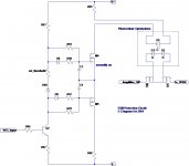
Protection Circuit
I've been studying some of the ideas from Esperado on amplifier protection in his ClassD project thread http://www.diyaudio.com/forums/digi...sures-class-d-system-project.html#post2731758. I'd like to incorporate some peace of mind when it comes to my speakers. The circuit I saw from Esperado looks very nice, but it is based on 4 opamps and I don't want to be looking to provide another set of power rails suitable for opamps.
I figure that I can reproduce part of the functionality with a discrete circuit. Just 1 transistor and some FETs to be exact.
The concept is to compare the input to the amplifier with the output from the amplifier. Taking into account the gain, the two should match. If they don't, something ain't good.
With an input cap on the amplifier there won't be dc comming in from outside. If there's dc generated by the amp, it will be visible as a difference between input and output.
The first step is to reduce the output signal by the gain of the amplifier so it can be directly compared with the input. This would normally require an adjustable element. However, I figure that the amplifier already performs this function for me. The input devices are already an error amplifier, comparing input with output. So I'll dispense with a copy of that and simply tap into the output from one of the amplifier input devices - or put it another way, I'll tap into the signal that feeds the VAS.
The next thing I need to do is boost that signal. So I make a clone of the VAS, and I do this as a single ended common emitter amplifier with simple resitor collector load. The output goes through an envelope detector - two diodes and then into a differential amplifier (you may recognize it as a Rush Cascode). I've used FETs because I need a high input impedance. I've set it up so that the Cascode is normally 'on' and switches 'off' when an error condition arrises.
An error condition causes a mismatch between input and output and consequently a large error signal appears at the output from the proection circuit VAS. This signal discharges the capacitors between the gate-source of the FETs and turns them off.
I've used a solid state relay to cut the output to the speakers.
thoughts ????
Attachments
Of course i'm interested by your idea. Few personal thoughts and remarks.The circuit I saw from Esperado looks very nice, but it is based on 4 opamps and I don't want to be looking to provide another set of power rails suitable for opamps.
I figure that I can reproduce part of the functionality with a discrete circuit. Just 1 transistor and some FETs to be exact. directly compared with the input. This would normally require an adjustable element. However, I figure that the amplifier already performs this function for me. The input devices are already an error amplifier, comparing input with output. So I'll dispense with a copy of that and simply tap into the output from one of the amplifier input devices - or put it another way, I'll tap into the signal that feeds the VAS.
The +- 12 V power rails of the protection can be used for other things, like soft power delays, remote power on, active filters, remote volume, in my case. So it just cost a little extra transformer and regulators.
I had too , of course, the idea to take the output signal (to be compared) directly from the feedback loop where it is perfect level and no tuning, as you said. It can be done in a new designed amp whith his own embeded protection. You just have to take great care to not add any parasitic capacities at this point where phases are critical. And to match the two inputs of your comparator up to the highest frequencies. Not so easy. (And i wanted my protection circuitry universal and independent from amps).
Taking the results directly from the output of the input stage of the amp does not satisfy me. I do not know what can happen if any faillure inside the amp (fist stage transistors burned in cut state, faillure from the power rails etc.) .. That why i wanted a completely independent system, even for it supply.
I will look further to your ideas, to see if i can stole one idea or two ;-)
Member
Joined 2009
Paid Member
I suspect phase shift errors are just one source of error. As Esperado points out, the non-linear load produces even more errors at the output. Fortunately, I don't think it matters because the protection circuit is looking for gross errors. I'm only expecting it to protect from dc output hurting the speakers, and a very low impedance load (a.k.a. short) which causes clipping. The circuit will trigger on clipping so it needs those capacitors, which in combination with the resistors in series with the diodes produces a low pass filter so that it isn't shutting the amp down on transients.
if the transients or the steady state waveforms are in phase and corrected/scaled to have the same amplitude then the detector/comparator circuit should not trigger............. so that it isn't shutting the amp down on transients.
Right. Not to forget that, if you tune your sensitivity to be at the limit, despite all internal phase errors, any additional little error will fire your protection. Tuned with an oscillo at full power, a little reduction in charge impedance will fire-up.. as well as the littlest clipping !!!!Fortunately, I don't think it matters because the protection circuit is looking for gross errors..
I am finishing the power part (delays) and i have added a gain stage after error detection for more sensitivity and easier tuning of it. It will be now for the all stuff (including power, soft start, and delay for the speaker on) one quad OP, and 3 comparators.
Coming soon...
Last edited:
Bigun,
congratulation on a such small PCB footprint of Yours TGM5 amp.
I see You use almost all semiconductor and other parts SMD, very nice. Can You refer to which SCH is based Yours SMD PCB artwork or post it here once more with parts names, which You chose, also sources would be of great help.
I wonder to try Yours SMD version and compare it to the non SMD version of the same SCH.
I vote for SMD.
Member
Joined 2009
Paid Member
Hi Sound_rays,
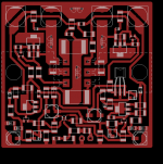
I'm pleased you recognized the challenge of designing a single sided pcb without jumpers !
I wanted to try SMD because I expect parts choices to be better, because closer placement of parts reduces trace lengths and because I can use a ground plane on the backside of the pcb.
If I were designing a commercial product this would be the WRONG way to do it. Double sided boards with plated through via's etc. are a much better option, allowing more optimal component placement without any real cost penalty. But for DIY, making double sided boards is more difficult and plated through holes are not really practical.
I am also using 2010 sized resistors. They allow me to run tracks underneath without needing fine geometry. The parts are easier to handle and are often marked with the value of the resistor. A commercial design would not do this. The smaller 0805 parts are cheaper, easier to obtain and take up even less space.
All my parts will be sourced from Digikey for my convenience. It means some parts that may have better performance may not be available to me.
I figure large sized SMD parts are nice way to DIY, no need to drill lots of small holes in a pcb and all the parts and wiring between them is clearly visible to me when I am debugging and measuring on the board.
The schematic is posted in this thread already - but I will post it again once I have decided whether to include a protection circuit.


Hi Begun, very nice board layout, congratulations. I have one comment though and that is regarding gluing transistor in the front end together.
I do not really subscribe to this from a practical point, it is theoretical. Mine is on opposite sides of the PCB and I have never bothered to match anything in any case but my off-set is minimal because I adjust off-set and bias at the expected operating temperature and re-adjust if necessary after a few ten minute intervals until it remains very stable.
Gain matching PNP and PNP over an operating range is practically not feasible and one will drift with respect to the other, besides the DC error in the NFB loop should take care of offset in any event.
Regarding pops and bangs during start-up should not be a concern either in a symmetrically balanced amp because it takes its zero reference from between the power supply caps and output will track this point from onset and zero current will be produced in the speaker.
Hi Nico,
As You stated I see this amp would be a serious candidate for use in an active speakers too
What would You suggest for a direct connection to tweeters ?
Would it be better to use an output relay delayed for xx sec. to stabilize ev. any possible o/p dc ofset or use a serial cap. to avoid dc.
Maybe OP relay would be a better solution to avoid capacitor ?
Regarding pops and bangs during start-up should not be a concern either in a symmetrically balanced amp because it takes its zero reference from between the power supply caps and output will track this point from onset and zero current will be produced in the speaker.
As You stated I see this amp would be a serious candidate for use in an active speakers too
What would You suggest for a direct connection to tweeters ?
Would it be better to use an output relay delayed for xx sec. to stabilize ev. any possible o/p dc ofset or use a serial cap. to avoid dc.
Maybe OP relay would be a better solution to avoid capacitor ?
- Status
- This old topic is closed. If you want to reopen this topic, contact a moderator using the "Report Post" button.
- Home
- Amplifiers
- Solid State
- TGM5 - all-BJT Simple Symmetric Amplifier