I am glad you like it. ")
It should be in all respect.
But TGM5 is better, in my mind.
It should be in all respect.
Member
Joined 2009
Paid Member
I like your SMD PCB very much, especially placement of the outputs, only a GND loop can be a potential interference generator.
I like this amplifier very much...
Thank you for the encouragement guys - it helps a lot to keep me going when there's a lot of distractions !
Im glad you found a solution, can you share it? I advice you to sim your Vbe multiplier, Vce change vs. Ic and plot the deviation. For Ic use real values plus variation in accordance to temp.
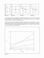
For my previous single ended VAS designs there's a bootstrapped-CCS load for the VAS so a better Vbe circuit was not needed. But in this symmetrical VAS design I see that the current is ill-defined in comparison. Fortunately, Hagerman looked at the impact of a varying VAS current through the bias generator; his solution is attached (figure 2d); it's simpler than a Sziklai multiplier but maybe not as accurate. I believe D Self has some similar ideas.
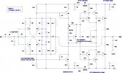
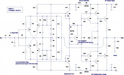
In my simulations I decided to vary the junction-temperature of all the small signal devices from a starting point of 40C up to 50C. For the main drivers, Vbe multiplier transistor and power devices I allowed the temperature of those to increase from 40C to 80C at the same time. The updated schematic is attached - the change is the addition of diode D5 and resistor R3. You might also see that I've added diodes to the power rails to better isolate the front end.
With the regular Vbe multiplier the voltage across the output emitters went from 58mV to 100mV. With the Hagerman multiplier it was more stable, varying from 60mA to 62mA over the same temperature range.
It's not sufficient to focus on tuning the Vbe multiplier to ignore the VAS current variations - you want to take full advantage and further optimize the value of resistors to produce for the smallest variation in bias over temperature. Some trial-and-error during the build would be ideal.
Attachments
Yes bigun that is the solution as I already stated here:
The curve d.) is exactly what we need here, multiplier Vout is constant regardless front-end bias variations, which is in this case inevitable. I agree that SSA resistors values have to be optimized to each stage quiescent current and power dissipation but that is normal procedure at new amp design.
Also the rail diodes are nice supplement for improving high ripple isolation-rejection.
Just continue and surprise us soon with some working pics.
P.S. What about circular GND connection on a PCB, do you think there will be no GND currents interferences?
Vbe multiplier has two major tasks to provide: it is there not only to sense the temperature from the output stage but also acts like a zener so the front-end bias variations have no influence to output bias conditions.
The curve d.) is exactly what we need here, multiplier Vout is constant regardless front-end bias variations, which is in this case inevitable. I agree that SSA resistors values have to be optimized to each stage quiescent current and power dissipation but that is normal procedure at new amp design.
Also the rail diodes are nice supplement for improving high ripple isolation-rejection.
Just continue and surprise us soon with some working pics.
P.S. What about circular GND connection on a PCB, do you think there will be no GND currents interferences?
Member
Joined 2009
Paid Member
Also the rail diodes are nice supplement for improving high ripple isolation-rejection.
One thing I've noticed - you have to be careful with this symmetric design. Being symmetric with dual power rails it tends to show very good PSRR because the ripply on the rails is equal and opposite. So you can get sucked into thinking that you don't need to worry too much.
But with Class AB the current pulses through the load flow asymmetrically through the power rails. If you have dual mono construction this is no issue. But I will have a common power supply for all 3 channels. This means that you can have high cross talk between channels even though PSRR for rectifier ripple is high. So the diode, resistor and cap in each rail are very necessary to isolate the front end of each amplifier. Ripple is the last of the worries
Just continue and surprise us soon with some working pics.
I'm afraid soon is not the way with my projects - kids, day-job, it tends to leave me time only for bits n pieces. My task this weekend is to place order with digikey for the parts.
P.S. What about circular GND connection on a PCB, do you think there will be no GND currents interferences?
Yeah, this needs some thought. I will have gnd plane on backside of pcb. I can place contacts from front side gnd bus to backplane with ease. But I don't want gnd currents from front-end of the amplifier using the gnd plane to return to the gnd connection by crossing the gnd plane undeneath power section - I prefer these currents to take the long route around the pcb as this is quieter. I'm not too sure on this one yet. If used properly, the gnd plane though, will prevent the circular gnd track on the top side forming a pick-up loop.
Last edited:
I'm doing an amplifier with a similar output stage. Your amp is interesting.
On the input part of your output stage, Q8 & Q9, you have the capacitor before the resistor, and then the resistor to the base. That's interesting, i've usually had the resistor first, then the capacitor as sort of a lpf. I'm wondering what the difference is, but if your amp is stable, I may try that. The CFP Triple amp I'm working on now stays cool, but has serious oscillation.
Is the intended use of your amp to drive full range mostly, or is subwoofer use good as well? I'm wondering what the benefits of CFP triple is besides the lower voltage drop, like if it has better drive than the darlington triple.
That input stage is wild. I really like it. I wonder besides PSRR how it really affects the sound. Keep it up, I know projects take time, as I feel my projects take too long and require lots of time, but it's SO worth it when it's done, it pays to be patient.
Member
Joined 2009
Paid Member
I'm doing an amplifier with a similar output stage. Your amp is interesting.
Thanks !
On the input part of your output stage, Q8 & Q9, you have the capacitor before the resistor, and then the resistor to the base. That's interesting, i've usually had the resistor first, then the capacitor as sort of a lpf. I'm wondering what the difference is, but if your amp is stable, I may try that. The CFP Triple amp I'm working on now stays cool, but has serious oscillation.
I went and checked where I put the cap/resistor on my TGM3 amplifier, which is where I first used this output stage and I can vouch that it is stable. I discover that I put a cap only on the negative pre-driver to keep the amp stable and I put it directly on the base-collector i.e. not before the base stopper resistor as I've drawn in this thread. I will amend my schematic - I think I prefer the idea that the cap goes directly from base to collector of the pre-driver.
I think it's common to require a cap to stabilize a CFP, avoiding it requires careful selection of the pre-driver and driver transistors together with pcb layout. I think the idea is to ensure that the pre-driver is a fast device and the driver a bit slower. I'm quite happy and prepared to use a good quality cap rather than rely on the properties of the devices.
Is the intended use of your amp to drive full range mostly, or is subwoofer use good as well? I'm wondering what the benefits of CFP triple is besides the lower voltage drop, like if it has better drive than the darlington triple.
I'm going to drive some multi-way floor standing speakers for my home theatre set up. They will be operated full range.
The CFP triple is a something I fond of. I see a number of benefits. The main benefit as I see it is that it's a triple. Being a triple you better isolate the high impedance VAS stage from the non-linear high current Class AB output and it's current swings and interaction with a non-linear load. The CFP is very linear because of the high (e.g. 40dB) local negative feedback loop around the pre-driver / driver pair. It has very good drive capability. I believe it has less phase shift than a Darlington.
That input stage is wild. I really like it. I wonder besides PSRR how it really affects the sound. Keep it up, I know projects take time, as I feel my projects take too long and require lots of time, but it's SO worth it when it's done, it pays to be patient.
The input stage you can credit to LazyCat. It has some nice features and some challenges, like all designs you gotta pick your tradeoffs. I never built a symmetric amp before and this one has a feature I like - the nfb is in two separate loops which lends it'self to a Hiraga-like harmonic distortion profile depending on how you set it up.
Last edited:
That input stage is wild. I really like it. I wonder besides PSRR how it really affects the sound.
SSA front-end is a wild animal in all respects.
It sounds fantastic, it is ultra fast and very stable. It is strongly referenced to GND from DC/AC aspect, so no unwanted distractions except the signal are possible.
Last edited:
Hi bigun
I am placing a lot of hope on you to test-built TGM5 very soon because I would really need two output transistors small amp module exactly like TGM5 PCB is. I would need 8 separate amplifier modules to make 4 amping to my horn speakers (4 horns per one channel). I would like to leave original passive crossover which is installed in each driver-horn case and supply each horn with its own amplifier channel. So for stereo I would need two separate amps each having 4 built in channels. Nominal impedance of each horn is app. 20 ohm, meaning to have much higher supply voltage but smaller output current. TGM5 with my Toshiba output transistors 2SA1987/2SC5359 can deliver 100Wrms per one pair, so for this power on 20 ohm load I would need something like +/-70V supply voltage which is realistic cause input pair is cascoded. I like small size of this PCB as it would be ideal for 4 channels amp in one case. Still I would have to built two of them ...
Please bigun hurry ...
Member
Joined 2009
Paid Member
I'm afraid my pcb won't necesarily be suitable to those kind of supply rails without some tweaking. You may have the input devices cascoded, but the VAS isn't. And there are other limitations such as capacitor voltages. Still, I'm impressed that anyone needs 100W rms x 8 for stereo horn speakers
Member
Joined 2009
Paid Member
Hi Hugh,
An excellent suggestion, it's a pity that Digikey doesn't carry them, or I'd grab some for TGM4. Really, there are some very nice devices out there. Indeed, for those wanting to build a high rail-voltage version of TGM5 this would be the way to go if not wanting to cascode the VAS devices.
An excellent suggestion, it's a pity that Digikey doesn't carry them, or I'd grab some for TGM4. Really, there are some very nice devices out there. Indeed, for those wanting to build a high rail-voltage version of TGM5 this would be the way to go if not wanting to cascode the VAS devices.
Member
Joined 2009
Paid Member
I have most of a parts list references to Digikey in place now.
And now that I have 'fixed' the Vbe multiplier to allow for stable output bias, I took a look at the VAS current variation with temperature and I believe I can fix this too with a very simple change.
Then I saw this:
I checked in my simulations - a 1 deg.C temperature imbalance between the input devices swings the dc-offset quite a bit (40mv - 50mV). It's a sensitive beast.
I am wondering if the front end of this design is adequate for a Class AB optimally biassed BJT output stage.
And now that I have 'fixed' the Vbe multiplier to allow for stable output bias, I took a look at the VAS current variation with temperature and I believe I can fix this too with a very simple change.
Then I saw this:
http://www.diyaudio.com/forums/solid-state/193923-simple-symetrical-amplifier-47.html#post2724672I can increase the offset from 5mV to say 150mV just by breathing over the input BJTs
I checked in my simulations - a 1 deg.C temperature imbalance between the input devices swings the dc-offset quite a bit (40mv - 50mV). It's a sensitive beast.
I am wondering if the front end of this design is adequate for a Class AB optimally biassed BJT output stage.

LC,
I don't think anyone thinks that..... I give credit where it's due, this is a mighty fine amp, and if Nico Ras shows interest, that absolutely confirms it.
Take credit, Andrej, but realise that many here are lurking, not commenting, but still very positive about it. I really think it's brilliant, and would encourage you.
Hugh
Member
Joined 2009
Paid Member
Lazy Cat - I'm counting on your DIY experience, I'm seeking your guidance. Shann's post came after mine by the way, but he's got stable bias now so I'm much encouraged.
You see, I'm trying to understand how the amplifier works, especially the bias and temperature stability. I have the feeling that this front end design excels with high currents.
I'm attaching a schematic with the latest tweaks. I've doubled up on the zener diodes, they're cheap enough and I can indulge in the concept of lower noise at the 5V to 6V range - I put two in series. I suspect the noise adds in quadrature too so that's even better. And if I want to experiment with lower Cascode voltage I can replace one with a short.
The resistors that provide current to the feedback node from the zener smoothed volage supply are now both trimmers. I know that only one is needed to set dc-offset balance, but with two I can also set the idle current through the VAS more easily. I've also put a resistor in parallel with each trimmer - to allow me to have a more sensitive trimmer adjustment (and using a high grade nickel thermistor here fixes the VAS current variations too!). Lastly, I've added emitter degen resistors to the Cascode devices. I did this mainly to facilitate my pcb layout - I have no use of jumpers that way and it's all single sided. But I also remember that such a resistor has been viewed as beneficial - something from the experiments done under the banner of memory distortion.
You see, I'm trying to understand how the amplifier works, especially the bias and temperature stability. I have the feeling that this front end design excels with high currents.
My bias is pretty stable after about 10 minutes, but I run the amp in "near class A" at just under an amp.Nico
What I'm trying to do is engineer it a but further for low bias outputs running in Class AB with Bipolar outputs. It's an evolving design - and that's part of the fun.My Iq is about 800mA, yes I run them hot but I find hot is good for two reasons 1) temperature is more stable and 2)harmonic distribution is a nice roll off starting with H2. Nico
I'm attaching a schematic with the latest tweaks. I've doubled up on the zener diodes, they're cheap enough and I can indulge in the concept of lower noise at the 5V to 6V range - I put two in series. I suspect the noise adds in quadrature too so that's even better. And if I want to experiment with lower Cascode voltage I can replace one with a short.
The resistors that provide current to the feedback node from the zener smoothed volage supply are now both trimmers. I know that only one is needed to set dc-offset balance, but with two I can also set the idle current through the VAS more easily. I've also put a resistor in parallel with each trimmer - to allow me to have a more sensitive trimmer adjustment (and using a high grade nickel thermistor here fixes the VAS current variations too!). Lastly, I've added emitter degen resistors to the Cascode devices. I did this mainly to facilitate my pcb layout - I have no use of jumpers that way and it's all single sided. But I also remember that such a resistor has been viewed as beneficial - something from the experiments done under the banner of memory distortion.
Attachments
Hi Gareth
I think components values optimization will bring enough thermal stability to SSA front-end, so VAS Iq current will be in +/-20% range. Output Iq is fixed with linear Vbe multiplier.
From my point of view for SSA TGM5 I suggest some basic rules:
- R3, R4 should be 100 ohm (bandwidth, stability)
- R13, R14 set the value for 2 mA of the input BJT's collector quiescent current
- R32, R33 should be omitted
- zener diodes lowered to voltage potential still ensure enough headroom for FB signal but not much higher, to limit the power dissipation of an input pair to minimum
- C3, C4, C9, C10 1000 uF
- C5 100 uF
Regards Andrej
Member
Joined 2009
Paid Member
Hi Andrej,
I'm thinking that the thermal matching of the input pair is going to be worthy of my attention. You suggested gluing together the two TO-92 packaged devices.
I'm wondering about an integrated solution, both transistors on the same piece of silicon in the same package, well matched they will track temperature changes together.
Attachments
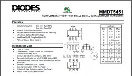
Very good choice.
Wow, now I know that this kind of dual complementary probably matched transistors even existing. Great.
But thermal connection in input pair only correspond to faster and more acurate offset tracking and have no influence to hFE temperature dependency, thus collector/VAS bias current stability.
Output DC offset stability is also good enough even now with normal plastic BJTs glued together (within +/-10mV).
The only way to complete front-end bias stabilisation would be by tracking mid FB bridge DC to Vbe change of the input BJT's - tough one.
Looking from your SMD PCB design aspect, this SMD complementary pair is just perfect.
Last edited:
Member
Joined 2009
Paid Member
I think the dc-offset stability AFTER the amplifier has warmed up is probably fine with glued TO-92 but I'm not sure about the start up of the amplifier when the temperature changes are the most significant - will my speaker cone be doing some dancing ? Of course, since I am using surface mount devices, I can't glue TO-92's together anyhow...
From your words you answered another question I was asking myself - why do Hfe matching ? - for LTP the matching affects the base bias current which affects dc-offset, but for this design it isn't relevant. So I don't see any need for Hfe matching.
From your words you answered another question I was asking myself - why do Hfe matching ? - for LTP the matching affects the base bias current which affects dc-offset, but for this design it isn't relevant. So I don't see any need for Hfe matching.
Gareth,
I have used these devices. You will need to use a special iron and a magnifying assembly to affix it to the pcb. For my tired eyes it has proven a nightmare...... strictly for machine assembly. I would urge you to simply superglue TO92s together, not quite as good electrically, but much more dissipation and much easier mechanically.
Cheers,
Hugh
- Status
- This old topic is closed. If you want to reopen this topic, contact a moderator using the "Report Post" button.
- Home
- Amplifiers
- Solid State
- TGM5 - all-BJT Simple Symmetric Amplifier