Using simulation for proof of concept.
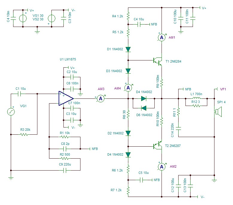
Lets build a circuit model that actually works.
Something that would actually drive 4 ohm loads
with 70 to 80 watts
Using a LM1875 that would never
dream of making so much power
Of course we can cheat a little with Ideal current sources.
But before you scream, its a simplified proof of concept.
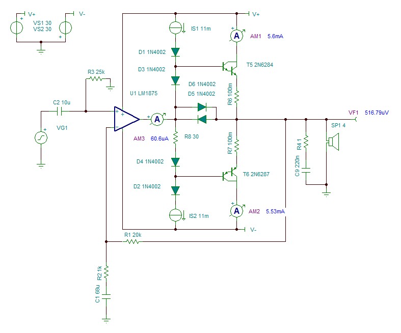
With 11ma current sources, D1/D2 would make sure they behave
D3/D4 provide basic diode drops for bias.
D6/D5 for the first time actually
provide current limit/short circuit protection.
R8 is set here, but would be adjustable for bias current
The transistors are finally turned on with a rather wimpy 5.5 ma of current
Using Darlington Transistors
DC analysis Below
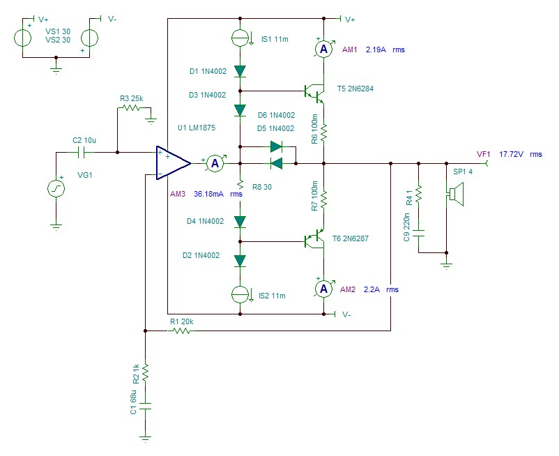
Looking at AC analysis
17.72 volts RMS into a 4 ohm load for 78.5 watts
The transistors now appear to be conducting current.
Around 2.2 amps of current.
Which is a significant improvement over the previous circuit
which was = 0
For a total of 4.4 amps AC
which makes sense since its 78 watts of power
Lets remove diodes D5/D6 and add the 2.7 ohm resistor.
Then Short the amplifier.
As you can see the 1875 clamps to the usual 4 amps as designed
DC offset rises like any amplifier and the external transistor
Fully shorts to 14 amps.
Which would likely instantly destroy it...
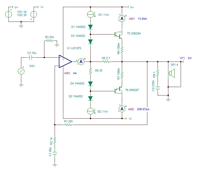
Now lets remove the pointless thing and replace them with
D5/D6 protection diodes
Now if you short the amp. LM1875 clamps to 4 amps as usual
and the external transistor also clamps to only 3 amps

Lets build a circuit model that actually works.
Something that would actually drive 4 ohm loads
with 70 to 80 watts
Using a LM1875 that would never
dream of making so much power
Of course we can cheat a little with Ideal current sources.
But before you scream, its a simplified proof of concept.
With 11ma current sources, D1/D2 would make sure they behave
D3/D4 provide basic diode drops for bias.
D6/D5 for the first time actually
provide current limit/short circuit protection.
R8 is set here, but would be adjustable for bias current
The transistors are finally turned on with a rather wimpy 5.5 ma of current
Using Darlington Transistors
DC analysis Below
Looking at AC analysis
17.72 volts RMS into a 4 ohm load for 78.5 watts
The transistors now appear to be conducting current.
Around 2.2 amps of current.
Which is a significant improvement over the previous circuit
which was = 0
For a total of 4.4 amps AC
which makes sense since its 78 watts of power
Lets remove diodes D5/D6 and add the 2.7 ohm resistor.
Then Short the amplifier.
As you can see the 1875 clamps to the usual 4 amps as designed
DC offset rises like any amplifier and the external transistor
Fully shorts to 14 amps.
Which would likely instantly destroy it...
Now lets remove the pointless thing and replace them with
D5/D6 protection diodes
Now if you short the amp. LM1875 clamps to 4 amps as usual
and the external transistor also clamps to only 3 amps
Attachments
I agree
At first I was fascinated for some reason with driving external transistors
With Chip amps.
The internet is full of rather simple circuits and it seemed like fun.
Its easier to build a discrete amplifier for more power.
I have always and still have a certain love for chip amps.
To have a little DIY fun.
The LM1875 is a 5 pin chip so it will always be a easy simple chip to play with.
I think the 5 pin package and lack of mute functions and dual pins for power
make it attractive to tinker with.
Keep in mind realistically with just the chip
A LM1875 thermally stays safe around 18 to 22 watts
So squeezing 70 watts with transistors just seems like fun.
LM3886 is rated for " 68 Watts"
But keep in mind again the thermal limitations which are well covered in the
data sheets.
The chip package is more realistically safe at around 40 watts.
The voltage tolerance of course is much higher.
So again I have designed external circuits, both BJT and Mosfet
where you can get up to 160 to even 280 watts with a LM3886.
But again I agree if you want a 20 to 40 watt amplifier
Then build a chip amp.
If you want 60 to 150 watts or higher.
Its time to look at Discrete Designs.
Then again its a hobby people spend thousands on fishing equipment
when you can buy a fish at the store for very cheap.
Sometimes we like the challenge or fun of a hobby.
Eventually it haunted me. I wouldn't sleep until I got
280 watts with a Chip Amp LOL.
I think its like old school computer chip over clockers.
Getting a chip up to ridiculous speeds with liquid nitrogen
you could never use.
Just to screen shot a over clock score before the chip exploded
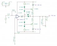
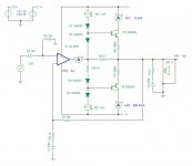
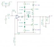
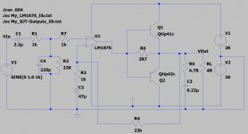
Of course post #121 is simplified
The model uses Ideal Current sources
and doesn't have proper power rail decoupling for stability.
Likewise could use the usual stability networks
on the output for difficult loads.
Un simplified for real world use.
With proper stability networks added.
R4 , R5 and C4 form basic bootstrap current source
in conjunction with R6, R7 and C5
obviously for clarity C4 and C5 connect to the amplifier output jumper
also marked as NFB for Negative FeedBack for the LM1875
With 60 volt Rails, Driving into clipping
54 volts into 8 ohms
52 volts into 4 ohms
78 watts 4ohm clean power around 92 watts 3% distortion
17.7 volts RMS 8 ohms shows same distortion rating as the chip itself
.01 % distortion
Attachments
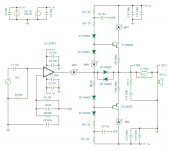
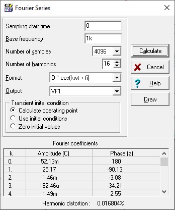
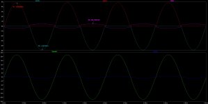
@WhiteDragon. That is very strange because the simulation I did in LTspice seems to be simulating the transistors turning on. You will notice in the Sim Traces image, that the transistors Q1 & Q2 collector current is measured at ±4.8A. The current measured through R6 is almost 459mA which is expected.
The simulation circuit used with the 2.7ohm resistor is shown in the schematic image. The transistors also seem to be heating up which indicates they are turning on.
The simulation circuit used with the 2.7ohm resistor is shown in the schematic image. The transistors also seem to be heating up which indicates they are turning on.
Attachments

Last edited:
As an addition to the above, in the LTspice simulations changing the value of R6 resulted in the below.
- Decreasing the R6 value to 1.5R increased the current flow through R6 to 798mA.
- Original R6 value of 2.7R resulted in a current flow through R6 of 459mA.
- Increasing the R6 value to 3.3R decreased the current flow through R6 to 378mA.
- Increasing the R6 value to 4.7R decreased the current flow through R6 to 268.7mA.
It tended to use 4R to reduce current of the opamp and resistor.
Anything higher than 4R can keep the chipamp protection from clamping
But due to anomaly of the circuit observed.
The topology frustrated me when it should be simple as expected.
Its why I moved to a different topology.
Which eliminated the resistor and the current it drops
And introduced bias and short circuit protection as shown in post 124
Doing basic DC analysis while bringing the amp up to 16.25 volts RMS
for 33 watts in 8R load
The chipamp shows 698 uV DC offset
The Transistors are basically off but the NPN sits slightly higher
NPN DC current is 8.02 nA ( off)
PNP DC current is 2.87nA ( off )
which is as expected
Not sure which spice sim your using but as per my latest post using LT Spice for my simulation the transistors do turn on and supply ±4.8A of current while a maximum of ±450mA peak. I have also attached the original Spice simulation plots.
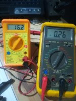
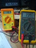
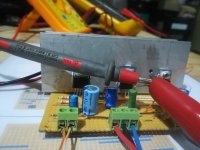
I have now run a real-world test on my prototype board as well. As you can see by the attached photos the amp is driving 16.2Vrms into a 7ohm load resistor while a measured maximum 260mA RMS is flowing through the R6 2.7ohm resistor. All other current is being supplied by the transistors so they are definitely turning on and supply the current.
Attachments

Last edited:
Images for above tests in post #128
These are the real-world test images for above post. You will see that the load of 7ohms is running at 15.7V at 2.37A and the current across R6 is 260mA. This test was done with a 23-0-23Vdc power supply.
Sorry for the two posts but I couldn't finish testing and uploading the images in the 30minutes given to edit the original post by the Admins.
Attachments
Last edited:
Are you trolling us?Doing basic DC analysis while bringing the amp up to 16.25 volts RMS
for 33 watts in 8R load
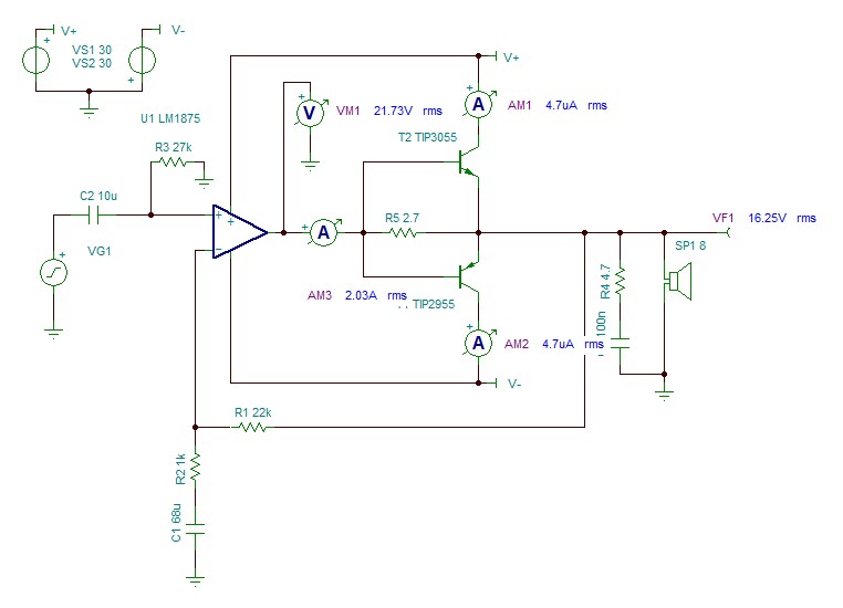
If you do AC Analysis
You will see what the 2.7 ohm resistor does.
True if the external transistors were actually on <--- THEY ARE
the opamp signal would reduce crossover distortion. <--WHICH crossover distortion??, the first 240mA come straight from TDA2030 with NO crossover distortion
Opamp output is 21.73 volts
but since there is a 2.7 ohm resistor in the way
Only 16.25 volts actually reaches the 8 ohm load. <-- there will never ever be 5.48V difference between Chipamp output and speaker voltage because you can NOT drop that much voltage across a BE junction. You even got the wrong units, for better analysis we use Peak Volts, not RMS. So your 5.48V RMS becomes actual 7.75V peak. STILL impossible Vbe drop.
Basically 2 amps of current from the opamp. <-- never ever. Chipamp will supply initial 240mA plus current needed to drive booster transistor bases. 21.73V RMS is actually 30V peak into the load (discounting drop across Vbe) so 3.75A peak, so Base current is 187mA so peak chipamp current is 428mA.
Note: I am Calculating, not Simulating, so my design is interactive.
I adjust Vbe drop to 1.8V peak so we have 29V peak available at speaker out, so 20.5V RMS, NOT 16.25 V RMS
Actually if the 2.7 ohm resistor was too high.
If you shorted the output of the amp. The opamp would not
go into protection. <-- gibberish
But since its shorted DC offset shoots way up to 9 volts <-- never ever ; 1.8V peak by datasheet
So then the external output transistors would finally turn on. <-- nonsense. They will turn ON as soon as R5 drops 650mV or so.
Well the NPN would turn on. <-- it was ON **way** before that.
And then blow up since the amp is shorted.
External transistor seem to be performing better than I expected.
Which is = Nothing WTF?
NPN 4.7uA AC current
PNP 4.7 uA AC current <-- nonsense. Under full drive as shown peak current acrossn each transistor is 3.5 AMPERES peak
as mentioned previously in the thread.
its better to use Darlington Output transistors
since it requires less current to turn them on. And also provide a bias network...so they actually turn on
They turn ON as soon as 650mVbe is reached
No simulator can give the nonsense values you post, which was already detected by Charlbur and B Force.
I can't help but wondering if it makes any sense.
EDIT:thanks Charlbur for taking the time and effort to verify and disprove this nonsense post, both in simulation and ACTUAL BUILD, which seems to be a rare gem these days
")
Last edited:
I moved to a different topology.
Which eliminated the resistor and the current it drops
And introduced bias and short circuit protection as shown in post 124
Once you get it this complex, to deal with the issues of the simpler circuit, it’s not really a chip amp anymore. You have a complete output stage, which you can graft any discrete front end onto. Chip amps have voltage limitations and you’re still stuck with that so 280 watts isn’t going to happen. You could configure the output stage to have gain (other things exist besides emitter followers) but that resembles a chip amp even less.
Original Project Objective
@JMFahey, I just couldn't understand where @WhiteDragon was coming from. It is a pleasure and at least we are assured the circuit does work.
@wg_ski, yes I agree with you 100%, the @WhiteDragon circuit is way too complex and defeats the whole point of the original post.
The original circuit and project posted in post #117 was meant to be a simple audio project that could be built on a piece of spare vero/project board if needed. It was never meant to be complex or ever will be audiophile quality. Although in simple listening tests the amp sounds reasonably good on a decent set of speakers and sounds far better than some other amps I have listened to.
As-built and tested with the measurements that were done in posts #128 & #129 prove the amp does work as expected. If you want to hear more of the audio from the chip amp coming through decrease the value of resistor R6. Increasing the value of R6, increases the voltdrop across the resistor and allows the transistors to switch on earlier as simulated in post #126.
Anyway, for hobbyists and those learning electronics just have fun building and testing this simple amp circuit! That's what it is all about anyway.
I have a Sansui set in storage whose schematic shows a STK module with it feeding big output transistors.
So in essence the chip amp is working as a pre or intermediate stage.
Here too same principle...just a variation of a very old theme.
Sansui B3000, late 1980s or early 1990s
So in essence the chip amp is working as a pre or intermediate stage.
Here too same principle...just a variation of a very old theme.
Sansui B3000, late 1980s or early 1990s
STK 3082-III in lower power version, B1000
STK 3152-III in higher power version, B3000
Sanyo lists them as Audio power amplifiers, the Sansui manual says differential amplifier.
Anyway, as mentioned above, the power output from this circuit is on the higher side for home use.
STK 3152-III in higher power version, B3000
Sanyo lists them as Audio power amplifiers, the Sansui manual says differential amplifier.
Anyway, as mentioned above, the power output from this circuit is on the higher side for home use.
Those types were designed to run external EF2 or EF3 output stages. Everything else included. Back in the old days, they were at least somewhat reliable with individual transistor dies mounted directly to the metal baseplate and wire bonded. Modern replacements use SOT23 and SOT223 soldered to a PCB and they quickly overheat and die. Some users have successfully made their own replacements using discrete parts and decent thermal management. Again, they really aren’t “chip amps” anymore. Real “chip amp STKs” had whole output stage too, and hooked up pretty much like an LM3886. Those tended to be less reliable because of the high dissipation output stage sitting on a thermal choke point and heating up, the whole front end. I wouldn’t touch modern versions with a 20 foot pole. SOT223 output transistors on a PCB - YEAH, RIGHT, that’s gonna work about 5 minutes before it explodes.
STK 3042-III series drives 2SB817/2SD1047 output transistors through 2SB631K / 2SD600K intermediate stage.
And they have written power amplifier on top of the datasheet...
And the circuit is like above.
So the use is the same, using a two stage (pre and intermediate stage) circuit to drive a high power stage.
A little confusing, direct output to speakers is not there, the 4141 series were connected to speakers. This STK series is different.
Anyway, driving a high power stage with a chip amp is a different approach, and it is easier to build a 49810 series amp, or use Mosfet based circuits driven by a regular pre amp to get the required output.
Last edited:
Not working with Hi Fi so no STK interaction but had to repair tons of Guitar amps using NLA TDA1514 (in Marshall and other UK brands), originally used LM3875/76/86 which are mutually pin incompatible (what were they thinking?) so every couple years had to redesign PCB , fed up with that I designed a *small* and very simple replacement amp using 5 transistors total: differential pair+Vas+couple TO220 Darlingtons (usually TIP121/126) which are on the edge of the stamp sized PCB and directly bolted to original chipamp heatsink so heat transfer is actually as good as on the original one.
A "universal" replacement since I couldn´t care less about original chipamp extra components which I don´t use, just bolt my miniboard on, and connect it, as you say, "like an LM3886"
I use it as a "black box" which gets signal and power and drives a speaker and only have 6 pins/pads to connect: IN hot and ground, Spk hot and ground, +/-V . Period.
Sorry, didn´t include a Mute pin .... do you think they'll flog me for that?
Has been saving my bacon for over 15 years now, is always available, repairable, and quite robust.
A "universal" replacement since I couldn´t care less about original chipamp extra components which I don´t use, just bolt my miniboard on, and connect it, as you say, "like an LM3886"
I use it as a "black box" which gets signal and power and drives a speaker and only have 6 pins/pads to connect: IN hot and ground, Spk hot and ground, +/-V . Period.
Sorry, didn´t include a Mute pin
.... do you think they'll flog me for that?Has been saving my bacon for over 15 years now, is always available, repairable, and quite robust.
The STK3042-III is a input and VAS only. What they write on the package has no relevance here. It will not function without a proper output stage.
Page 1 of the datasheet has the internal schematic and there's no output arrangement, and page 3 has the actual implementation where the external output stage is quite clearly drawn.
STK3042III Datasheet PDF Download - SANYO -> Panasonic
Page 1 of the datasheet has the internal schematic and there's no output arrangement, and page 3 has the actual implementation where the external output stage is quite clearly drawn.
STK3042III Datasheet PDF Download - SANYO -> Panasonic
- Home
- Amplifiers
- Chip Amps
- TDA2030 with transistors