Bricolo said:
I know that pin4 is activated in the TDA1541A, since it is the right channel digital input, when set up in simultaneous mode.
What I wanted to know, is if the pin4 can be used as a SCK input when the DAC is set up in I2S mode.
Thanks
Alex
I think so. Pin 2 & 4 could be strapped together while SCK is connected to pin 2.

ZERS said:
I think so. Pin 2 & 4 could be strapped together while SCK is connected to pin 2.
With TDA1541 pin4 is SCK in I2S mode, clocking the output latch.
With TDA1541A pin4 is nothing in I2S mode, i've connected it to dgnd in my dac and i still here music
Regards,
Well, to sum up :
I2S -----> TDA 1541A
EF ----> DGND
SCLK ----> PIN 2
WCLK ----> DGND
DATA ----> PIN 3
GROUND ---> DGND
V4 ---> DGND
Pin 27 & 28 ---> +5V
What about PIN 1 ???
Regarding the PIN 4 of the TDA 1541A it's either DGROUND or SCLK as well.
The 1541A datasheet says DGND
I2S -----> TDA 1541A
EF ----> DGND
SCLK ----> PIN 2
WCLK ----> DGND
DATA ----> PIN 3
GROUND ---> DGND
V4 ---> DGND
Pin 27 & 28 ---> +5V
What about PIN 1 ???
Regarding the PIN 4 of the TDA 1541A it's either DGROUND or SCLK as well.
The 1541A datasheet says DGND
ZERS said:
I think so. Pin 2 & 4 could be strapped together while SCK is connected to pin 2.
ZERS: pin 4 in the non A version is SCK
for the A version in IIS mode, it's not used (officially) and should be connected to ground and not to BCK (pin 2) (it's not the same as SCK)
And I don't know what you was reffering to in your last post, but it seems wrong. IIS has 3 signals (BCK, WCK and DATA), there's no SCK in it. (neither EF or V4)
Bricolo said:
ZERS: pin 4 in the non A version is SCK
for the A version in IIS mode, it's not used (officially) and should be connected to ground and not to BCK (pin 2) (it's not the same as SCK)
And I don't know what you was reffering to in your last post, but it seems wrong. IIS has 3 signals (BCK, WCK and DATA), there's no SCK in it. (neither EF or V4)
I'm refering to the CDPRO2 datasheet (a philips drive) that could sent I2S to a DAC chip.
Unfortunatly, the datasheet is too big to be attached

Here is a part of it :
IS2 output :
PIN1 : EF : C2 error flag
PIN2 : SCLK : serial clock
PIN3 : WCLK : world clock
PIN4 : DATA : data
PIN6: GROUND
PIN7: V4 : versatile output
ZERS said:Well, to sum up :
I2S -----> TDA 1541A
EF ----> DGND
SCLK ----> PIN 2
WCLK ----> DGND
DATA ----> PIN 3
GROUND ---> DGND
V4 ---> DGND
Pin 27 & 28 ---> +5V
What about PIN 1 ???
Regarding the PIN 4 of the TDA 1541A it's either DGROUND or SCLK as well.
The 1541A datasheet says DGND
ZERS said:
I'm refering to the CDPRO2 datasheet (a philips drive) that could sent I2S to a DAC chip.
Unfortunatly, the datasheet is too big to be attached
Here is a part of it :
IS2 output :
PIN1 : EF : C2 error flag
PIN2 : SCLK : serial clock
PIN3 : WCLK : world clock
PIN4 : DATA : data
PIN6: GROUND
PIN7: V4 : versatile output
As said here, the TDA1541(A) can only handle BCK, DATA and WS.
So i think it is:
DATA->DATA
SCLK->BCK
WCLK->WS
GROUND->GROUND
But that is without looking at the datasheet. The other pins are OUTPUTS, so leave them NOT CONNECTED, unless you want to
 your CDPRO
Henk, thanks again for your posts, I consider them very valuable.
Interesting note about pin 28.
Pedja
I guess it is no problem to have the same delay for all the lines but you will not have the same delay for all the frequencies. Honestly, I do not have an idea if this could be bad or not, just want to note that the general 10ns becomes some 9.7ns on 2.8MHz and 8.6ns on 6.4MHz.HtP said:Delay is not important as long as the delay is equal for all inputs.
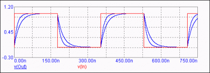
I was not referring to the noise/resistor induced jitter, I was referring to the smoothed waveform like generally less wanted waveform here because of the problem of indeterminacy of the moment of transition in time. Attached are the bandwidth unlimited ~2.82MHz square and squares limited wit RCs of 12ns and 22ns. Are there good reasons why they usually use just square signals here or not? Or the rise time is all we need to determine the best bandwidth of these squares?Delay has no influence on the definition of the transition as long as the noise of the delay element or the noise of the inputstage does not significantly cause jitter.
I do not quite figure this. Three or 4 active divider pins are inside -15V- -5V range but the others are not.Current reference generator for the output current is between -5V and -15V. Output current from the dac comes out of pin 6, 25 via diode switches or comes out via the +5V pin 28 by darlingtons. This means that complementory output signals L+R flow in supply pin 28.
Interesting note about pin 28.
Pedja
Attachments
Bernhard said:If 1541 and 1541A are different, why can I plug 1541 in a player that was made for 1541A, and plug 1541A in a player that was made for 1541 ?
Please read datasheets how 1541/7220P/A are connected and compare with 1541A/7220P/B schematic. Hint : 470 pF.
Please read datasheets how 1541/7220P/A are connected and compare with 1541A/7220P/B schematic. Hint : 470 pF
Which datasheet to look in? TDA1541 or SAA7220?
I have to find out why my Philips CD 304MKII doesn't work when I exchange SAA7220P/A for P/B version.
This might have something to do with that 470p cap.
Bartek
Bernhard said:If 1541 and 1541A are different, why can I plug 1541 in a player that was made for 1541A, and plug 1541A in a player that was made for 1541 ?
And because philips probably connects pin 2 and 4 in players with 1541A. Not needed, but also not harmfull
 Or is it...?
Bricolo said:I think it's in the 7220's datasheet, since there's nothing about it in the 1541's
But the datasheet I have has nothing about the differences betwaeen A/B version
The doc floats around here. Search and you will find it (mosted it myself few times i think). Its about A/B/C
The doc floats around here. Search and you will find it (mosted it myself few times i think). Its about A/B/C
I remember reading it,but don't remember any info about diffrent connections and/or caps.
Bartek
Ok
Here we go again. The 470pF is the DEM cap on the 1541A.
It's 470pF in the datasheet, in real life 680pF is used (also?).
Pins 16/17 are NC on the 1541 (officially, but they are connected anyway i think). The cap is not needed there (internal?).
So:
1541: pin 4 = SCK, no DEM cap
1541A pin 4 = nothing, DEM cap.
So 1541 in 1541A player should not work, since pin 4 is not connected.
So 1541A in 1541 player should not work, since DEM cap is not
there.
But both work...
So in 1541A player pin4 is connected to 2 anyway
So in 1541 player there is a cap on pin16/17
And yes, in my 650 (7210/1541) there is a cap
Aren't we dutch some funny guys
Guido,
I have just read one of your older posts when you tried to exchange older M4804A chip in your CD 650 for SAA7210.
Did SAA7210 work as a direct replacement,or there were some diffrances?
I have the player with that old chip and have some spare SAA7210 to drop in.
Bartek
I have just read one of your older posts when you tried to exchange older M4804A chip in your CD 650 for SAA7210.
Did SAA7210 work as a direct replacement,or there were some diffrances?
I have the player with that old chip and have some spare SAA7210 to drop in.
Bartek
- Status
- This old topic is closed. If you want to reopen this topic, contact a moderator using the "Report Post" button.
- Home
- Source & Line
- Digital Line Level
- TDA1541 info