I am trying to build the amp on TAS5630 also, but I use 64-Pin QFP (PHD) version of this chip. This package is a lot thinner (1.5 mm approx), but it has wider legs and allows to develop good layout easier... For example, it allows to place the vias near to GND legs of chip, to get the all advantages of the ground plane. And it may be done NOT under the chip, but near to it's border, using some piece of wire, mounting it in through-hole manner.
Last edited:
 that would be nice
 Tas5630+SMPS module wear the new coat in new year!
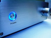
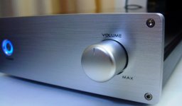
I put new aluminum case on TAS5630+SMPS module few days ago,looks good,New Year coming!I think this treasured object should wear new coat in new year.
I put new aluminum case on TAS5630+SMPS module few days ago,looks good,New Year coming!I think this treasured object should wear new coat in new year.
Attachments
Last edited:
Yes the it is, but at the time i was working on this the QFP version was still in development.
News??
some problem
have you MSN i have same problem on TAS5630 ,it has cost me long time to save it ,but until now i have not get the ouput signal ,by the way 4 chips i have burned my mail feng4456@yahoo.cn wish your help
I have decided to try and make a homemade D-Class amp useing the new TAS5630 chip from Texas Instruments.
The specs on it are amazing like total output power 600W, low THD (0,03%) single supply 20-50V operation, differential analog inputs.... and on top of it all its almost as simple to use as a AB class chip amp.
So all this made me decide to try and build one of them.
Right now i have a PCB made in eagle for the HSSOP version of the chip( The TQFP version i wanted is not in production yet) and i just recently got the chips them selfs .As you can see i am using the BTL mode of it that has a max of 300W but the high power is mealy to provide headroom and keep the amp cold.
On the PCB the 4 holes you see are not for the purpose of mounting the PCB but they are 775 CPU socket push pin heatsink mountings. I just toght why not simply use a CPU heatsink to cool this. As for the white you see around the board thats the solder mask stop layer so i can cover those in solder to provide a better connection in the high current paths.
have you MSN i have same problem on TAS5630 ,it has cost me long time to save it ,but until now i have not get the ouput signal ,by the way 4 chips i have burned my mail feng4456@yahoo.cn wish your help
Hi Berni8k, I like your product. Could you send me an e-mail: vincentbeck@seznam.cz any material on this amplifier with TDA5630? I would like to make this as my bachelor's thesis and your diagram and PCB design in the EAGLE program would help me much.
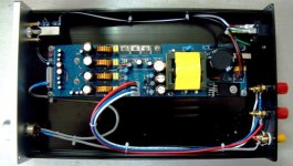
Hi berni8k,Here is the final version of the PCB that uses ground and power planes on the 2nd layer.
would you be so kind to us, who like to build this amp, and serve us with your already made schematics?
Thanks
interleaved flyback smps for tas5630
some friends asked us for higher power level stage for 4ch 2pcs tas5630 amp, cost must lower ,800w rms power , any friends here tried interleaved flyback smps for this power level? TI FAE engineer suggest us try ucc28061 and send some files to us, if anybody here have experiences of this , pls tell us, we have finished ucc28061+LLC +2xTAS5630 board years ago, works well, but cost higher.
TI ucc28061 led drive evm
bbs.dianyuan.com/bbs/u/84/3861261708762.pdf
other reminder,tas5630b datasheet have revised its value , 400w for PBTL mode,
in other words , it can works well at 400w rms power level, we have declare this years ago, but we have to call it 600w level, because if set as 2ch mode, it can delivery out 300w each channel, attention! this value mean only one channel loaded and tested,the other idle at this condition.
if use it as audio equipment , it is enough, because audio signal only occupy 1/8 rms power when playing, 300w each provide very good dynamic range each channel,only forbid to add continuous 600w loader for both channel.
so if design it as hi-fi amp 600W declare value no problem, if use it as pro type you have to declare 400w rms power.we have enough experiences to cut off error like chip burnt /reset latch/50v peak voltage destroy.
Last edited:
- Status
- This old topic is closed. If you want to reopen this topic, contact a moderator using the "Report Post" button.
- Home
- Amplifiers
- Class D
- TAS5630 D-Class build