Is there a good explanation why an isolated ground can be a problem here? Excuse my limited knowledge...
but DC/DC's are inherently worse because of their isolated grounds on input and output, those make nice dipole antennae.
...
")
Just have seen the 2W Recoms are about 23 Euro per piece @ Conrad shop. So it would be much cheaper and better (EMI/RFI) to use the simple analog circuits.
Well, euhm, the fact that there are 2 area's that do not form a single plane allows voltage difference between them. I've seen voltage spikes as big as 8V between ground planes (that's in power electronics, you can't measure this, but the amplitude is derived by the fact that there are parasitic gate turn-on's). 2 traces or planes that are physically separated and at different potentials make an antenna.
If that EMI (which is broadband in the case of a DC/DC) gets demodulated then it can and will be audible.
If that EMI (which is broadband in the case of a DC/DC) gets demodulated then it can and will be audible.
...fits to my expectation. It won't provide the DC accuracy which can be achieved by the solution of the first pic with a shunt regulator as reference and OP amp loop perfection, but nobody needs high DC accuracy for a OP amp supply. Noise figures should be fine also in the simple approach.I've seen the right DC supply filter before and it works just fine.
Good to hear that this is already a proven solution, because when I had this idea some years ago I only had build and measured the Rolls Royce version on the left.
..well, of course one could even ask: Who needs a low noise supply at all for OP amps?
==> Some luxury of doing it better than necessary is allowed even in the LiteAmp.
(Spartanic builders have the option to keep out the feedback cap and jumper two resistors in order to achieve the boring standard supply circuitry.)
DC/DC converters... Well, it is possible to do it right - but one might have to search for the right type. A blind choice likely would not provide low interference to the audio. In any case, as already mentioned by astx, it would cause a heavy cost adder with a hard to get device - which would be contradictive to the fundamental idea of the lite amp. The lite amp is intended as an affordable high quality design with only few hard to get components. And these few key components I intend to offer in a set at a non profit price.
Limiter Stage
The gain board is intended to become an universal input gain stage with optional limiter function and optional offset adjustment.
This gain board should be usable for any amplifier which needs an input gain stage and/or limiter
Hello Chocoholic
greetings is it possible for you to post gain stage limiter schematic if possible i would like to make it for my AB class amp
warm regards
andrew
Hi Andrew,
yes, I intend to fully disclose the schematic and hints of the gain board.
Please note that it is not ready yet and also the first schematics might be for discussion and collecting wishes from the community- not ready for building.
The post which contains a package of data for buidling will be clearly be highlight as a builders package.
Here is the first schematic of the gain stage with limiter for discussion.
Not build yet, only theory so far, not tested.
The input stage with U102 is a low noise differential input gain stage with an input impedance of 100k and input protection up to 50Vrms.
This part hopefully won't make to much surprises.
Similar I guess with the Sallen Key Low Noise Supply.
More demanding is the limiter.
U101 is a Vactrol (LDR+LED) which attentuates the signal in case of to high input levels.
U103 is a TL074 which forms the control mechanism of the limiter.
This circuitry offers a very high compression rate of more than 40db and at the same does not cause a dynamic compression and does not pump much. Dynamic compression is simply avoided by a long release time.
The threshold of the limiter is a dynamic threshold which follows the rail voltage of the power amp and limits the output to 90% of the rail voltage.
Basically the design should be fine for rails from +/-20V up to +/-100V.
The shown values would fit for VTL5C2, however in reality I intend to adjust it to the more common NSL32. This is likely to require changes in the lead compensation (C109) and proportional loop gain setting (R128 & R129), and potentially also in attack time and release time (R134, R130, C110).
The lead compensation compensates the slow dR/dt of the VTL5C2 and is neccessary to allow high compression rates with fast attack times at the same time without overreaction of the limiter.
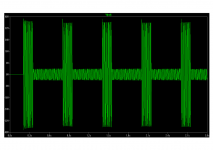
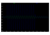
The first simulation screen shows the operation with an input signal which would already force the amp 6db to high (double voltage) without limiter and would result in heavy clipping. The recurring bursts simulate a music program with 100 beats/min.
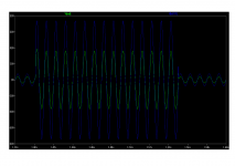
The second simulation screen shows a zoom of the output signal with limiter (green) and for comparison the signal which would correspond to the input signal without limiter.
With 6db to much input signal the limiter easily keeps the amp output unclipped.
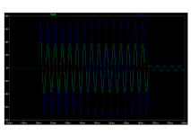
The third simulation screen shows a zoom of the first burst after a long period of silence. Imaginge music was off and you tip on PLAY at the CD player while the volume is turned up too high...
Even under this condition only the very first half wave gets slightly clipped, then the limiter already reduces to unclipped.
The fourth simulation screen shows a zoom of recurring beats with 10 times of the possible level. Means the input signal would demand the amp to deliver 370Vp...., without limter the output signal would become a fully clipping rectangle.
Also here the limiter keeps the signal low enough to show just minor clipping during the first waves of each burst and then runs unclipped.
So far so good. Well will see if also reality knows how it should behave.
Also you can post special wishes from your side.
The layout is not yet started, so I will check if/how your wishes could be added.
Not build yet, only theory so far, not tested.
The input stage with U102 is a low noise differential input gain stage with an input impedance of 100k and input protection up to 50Vrms.
This part hopefully won't make to much surprises.
Similar I guess with the Sallen Key Low Noise Supply.
More demanding is the limiter.
U101 is a Vactrol (LDR+LED) which attentuates the signal in case of to high input levels.
U103 is a TL074 which forms the control mechanism of the limiter.
This circuitry offers a very high compression rate of more than 40db and at the same does not cause a dynamic compression and does not pump much. Dynamic compression is simply avoided by a long release time.
The threshold of the limiter is a dynamic threshold which follows the rail voltage of the power amp and limits the output to 90% of the rail voltage.
Basically the design should be fine for rails from +/-20V up to +/-100V.
The shown values would fit for VTL5C2, however in reality I intend to adjust it to the more common NSL32. This is likely to require changes in the lead compensation (C109) and proportional loop gain setting (R128 & R129), and potentially also in attack time and release time (R134, R130, C110).
The lead compensation compensates the slow dR/dt of the VTL5C2 and is neccessary to allow high compression rates with fast attack times at the same time without overreaction of the limiter.
The first simulation screen shows the operation with an input signal which would already force the amp 6db to high (double voltage) without limiter and would result in heavy clipping. The recurring bursts simulate a music program with 100 beats/min.
The second simulation screen shows a zoom of the output signal with limiter (green) and for comparison the signal which would correspond to the input signal without limiter.
With 6db to much input signal the limiter easily keeps the amp output unclipped.
The third simulation screen shows a zoom of the first burst after a long period of silence. Imaginge music was off and you tip on PLAY at the CD player while the volume is turned up too high...
Even under this condition only the very first half wave gets slightly clipped, then the limiter already reduces to unclipped.
The fourth simulation screen shows a zoom of recurring beats with 10 times of the possible level. Means the input signal would demand the amp to deliver 370Vp...., without limter the output signal would become a fully clipping rectangle.
Also here the limiter keeps the signal low enough to show just minor clipping during the first waves of each burst and then runs unclipped.
So far so good. Well will see if also reality knows how it should behave.
Also you can post special wishes from your side.
The layout is not yet started, so I will check if/how your wishes could be added.
Attachments
Last edited:

Hi Toni,
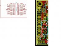
yes, the pinning of the connector from main to daughter board is fixed.
Please refer to the attached picture of this post.
The picture shows the pinning (top view) of the mother board.
The pinning of the daughter board must be the same, considering
it to be turned vertical and having the components on the outside.
The connector is 12x2.
Grid: 2.54mm.
Center of pin 1 is in 11mm distance from the upper board edge.
Center of pin 23 is in 10.9mm distance from the lower board edge.
Voltage gain of the main board is 4.8 (+/-40V type).
Inverting.
Cheers
Markus
Attachments
chocoholic,
have you considered monitoring the comp pin to control the limiter ?
another idea to reduce the dissipation of the regulator is to use a small cap from the classD full swing signal into 2 diodes as a charge pump.
a small series resistos needs to limit the current peaks
have you considered monitoring the comp pin to control the limiter ?
another idea to reduce the dissipation of the regulator is to use a small cap from the classD full swing signal into 2 diodes as a charge pump.
a small series resistos needs to limit the current peaks
This node is inside the control loop which also partially compensateshave you considered monitoring the comp pin to control the limiter ?
the slow output filter. In the frequency domain you will find mostly inverse transfer function of the output filter.
Means the signal at this point will contain pretty some misleading information towards high frequencies.
Additionally at this node the triangular carrier signal is larger than the audio.
Last but not least it will show all error correction activities of the loop.
Basically it would be possible to monitor this node, but the likelyhood of
mistriggering the limiter would be high.
Also it would not be an universal solution for other amp.
True. Well established in SMPS and other electronic control gear.another idea to reduce the dissipation of the regulator is to use a small cap from the classD full swing signal into 2 diodes as a charge pump.
a small series resistos needs to limit the current peaks
However in the LiteAmp it would cause an undesired side effect.
Plopping during turn ON, because the rails of the gain board would ramp
up slowly after the main amp is already active.
The current design starts without plop, because all rails and many operating points are stable before I activate the half bridge. After the halfbridge starts only the OTA with the loop gain network has to settle, this happens very calm & fast with just a silent 'tick' on the speaker.
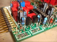
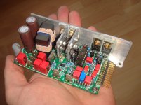
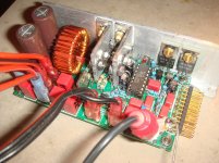
Mainboard PCB assembled
Assembled and everything is fine.
Mechanical construction is proper on paper, also proper in reality.
But paper tends to hide how tight the heat sink construction
will appear during assembly. Assembly needs some patience and mechanical
skill.
OCP (which was not present in my earlier bread board) is set to 30A peak.
This ensures plenty of headroom for operation at 2R from +/-40V rails.
With respect to an earlier request I also changed the output inductor from 12uH to 15uH.
==> Ok, found a good adjustment for this as well.
Furtheron 15uH causes less continuous stress to the e-caps, so I decided to pick the 15uH as preferred value for the +/-40V version.
Experiments with various different choke types show that a T106-2 with 33turns is a good choice, but also other solutions will work.
Attachments
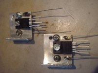
Opinions on how to mount torroids for good EMI are somewhat diverse.
Once I tried to measure the leaking fields with a loop probe and found
similar amounts in all directions. Laying it horizontal might be helpful, because then theoretically more of the leaking fields can be caught by the GND plane, reducing the radiated emissions. On the other hand theoretically this might increase the conducted emissions....
In fact I never made proper measurements on this topic, neither for radiated nor for conducted EMI. However the shown build appears to be reasonably calm with respect to ordinary FM receivers.
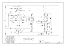
System schematic for the main board of the LiteAmp:
Well, on system level there is the schematic in the first post.
If you are curious for a schematic showing all components in detail - I am still reluctant. But of course everybody who wants to build the amp can get
the PCB + set of key components + BOM + building hints for a non profit price. - Will settle the proposal when also the gain board is ready.
Well, and then there is no way to avoid reverse engineering.
But I do not want to make it too simple for the commercial copy cats from the very beginning.
Potential later publication of details will depend on my feeling if the amp is popular enough in DIY circles.
Once I tried to measure the leaking fields with a loop probe and found
similar amounts in all directions. Laying it horizontal might be helpful, because then theoretically more of the leaking fields can be caught by the GND plane, reducing the radiated emissions. On the other hand theoretically this might increase the conducted emissions....
In fact I never made proper measurements on this topic, neither for radiated nor for conducted EMI. However the shown build appears to be reasonably calm with respect to ordinary FM receivers.
System schematic for the main board of the LiteAmp:
Well, on system level there is the schematic in the first post.
If you are curious for a schematic showing all components in detail - I am still reluctant. But of course everybody who wants to build the amp can get
the PCB + set of key components + BOM + building hints for a non profit price. - Will settle the proposal when also the gain board is ready.
Well, and then there is no way to avoid reverse engineering.
But I do not want to make it too simple for the commercial copy cats from the very beginning.
Potential later publication of details will depend on my feeling if the amp is popular enough in DIY circles.

Assembled and everything is fine.
Mechanical construction is proper on paper, also proper in reality.
But paper tends to hide how tight the heat sink construction
will appear during assembly. Assembly needs some patience and mechanical
skill.
OCP (which was not present in my earlier bread board) is set to 30A peak.
This ensures plenty of headroom for operation at 2R from +/-40V rails.
With respect to an earlier request I also changed the output inductor from 12uH to 15uH.
==> Ok, found a good adjustment for this as well.
Furtheron 15uH causes less continuous stress to the e-caps, so I decided to pick the 15uH as preferred value for the +/-40V version.
Experiments with various different choke types show that a T106-2 with 33turns is a good choice, but also other solutions will work.
Great work I like the form factor.
Is this a open source project or a commercial project?. any how I have a small 8-inch sub-woofer project I want to undergo this seem to fit the my need very well.
You will hate it during assemblyI like the form factor.
- Home
- Amplifiers
- Class D
- SystemD LiteAmp