Hi gommer,
a few side posts are Ok, but if you intend to go for a fundamental
and extensive discussion of the IRS2092 and how to simulate and use it,
then I would ask you to open a dedicated thread.
Your model of the IRS2092 is pretty much reduced to the very minimum.
And you are absolutely right, the data sheet either hides one further polarity inversion or has mixed up the comparator inputs.
Your SIM is a good starting point and you can extend it step by.
-I.e. dead time mechanism
-Clipping effects of the OTA for current and voltage
-Bandwidth of the OTA ( forget the data sheet for this)
-Level shifter/drivers
-Short comings of the real device which you might not find in the data sheet,
but by your own measurements only.
The caps in the signal path would also remain wired.
I dislike the ceramics in the signal path and experiments with small film/foil SMD, say 0805 and 1206, showed that it is hard to solder them without damage (large film/foil SMD where less critical).
Why do you dislike ceramics??
For small values like 1nF or less in the signal path (or tuning), NP0/C0G are near perfect caps ....
For output and input film are of course better suited, with larger voltages, and larger values .... and yes SMD types do not seem to offer much advantages here
Best regards Baldin
Hi Markus,
Rest assured, I won't mess up your thread and a big thank you for the confirmation. As this was really my very first attempt at class D simulation, I was looking for the confirmation to go further from this point. Which is exactly what you did. Thanks a lot.
Cheers, Marc
Rest assured, I won't mess up your thread and a big thank you for the confirmation. As this was really my very first attempt at class D simulation, I was looking for the confirmation to go further from this point. Which is exactly what you did. Thanks a lot.
Cheers, Marc
For small values like 1nF or less in the signal path (or tuning), NP0/C0G are near perfect caps ....
There are multiple people reporting that NP0/COG measure fine, but sound harsh. One of these persons I know and had listening tests with him for other topics. He really could easily (on the first few tones!) seperate two amplifiers in blind...
Regarding the NP0/COG I have no personal tests done, but tend to trust in the reportings.
On the other hand there are five caps which would be obvious candidates for SMD size 1206 NP0/COG and of course it would help for the layout.
Poll:
The said five caps in the small signal area are in the value range below 10nF.
Up to now I intend to foresee footprints which suit even the wired WIMA FKP2 types. These footprints hopefully are large enough to experiment with multiple other brands and types according users preferences.
Options to save space:
a) Changing to wired MKT
b) Changing to NP0/COG
Options a&b could be splitted even further by taking care which caps define transfer functions inside the audio band - or less critical caps which have their mayor influnce only above the audio band.
Please let me know your views, especially hard NoGo-opinions and prefering a larger PCB rather than allowing NP0/COG.
In first step for sure I will try to enable the layout for the FKP2 footprints.
Kemet has a short document about: Microphonics / MLCC
The recommendation is to use class I dielectric (=NP0/C0G) to reduce/avoid microphonic effects.
The recommendation is to use class I dielectric (=NP0/C0G) to reduce/avoid microphonic effects.
MLCC is just naming the construction of multilayer ceramics. It is very unspecific and in terms of electrical specification and microphonic behavior it can be anything.
Still it would be interesting to get a link to the types which are promoted for audio applications.
COG/NP0 like astx says specifies the zero temperature coefficient.
But there is more behind, COG/NP0 is a sub group of the class 1 cluster of capacitor ceramics. ...more details to this clustering should be somewhere in EN 60384 or EIA RS-198...
COG/NP0 is usually based on TiO4 with some adders. It offers a very low dependency of capacity on the voltage (==> low distortion) and low losses.
Very different for example X7R. X7R is a sub group of the class 2 cluster and the commomly used materials have not just higher losses, but unpleasant high derating of capacitance vs. voltage (==> distortion).
Even worse then in class 3 ceramics.
The main downside of NP0 is the comparably low permitivity, which limits the
achievable capacitances for a certain size.
Here class 3 ceramics excel.
Costwise - yes there are also differences, but nothing which would be a show stopper for DIY.
FKP2: Glad to find agreement here. Besides the data sheet also my personal experience with this type is fine and I have added it as a standard choice in my DIY component boxes.
Note:
The described classes are not linked to the protection classes of the safety standards, despite the fact that also specific capacitor types X2, Y2, Y1... exist, which are linked to safety standards.
Last edited:
...still some work to do, and it is going to be pretty crowded.
Changed the orientation of the IRFIs again to the same like on my breadboard.
The trial to have them at the edge of the PCB for easy heatsinking was pure pain for the parallel connection of both IRFIs.
The position in the middle will need two angular pieces as thermal link, but in class D the electrical requirements of the PCB clearly has higher prio than easy heat sinking.
Attachments
Actually, I'd suggest using this thread over opening a new one as it has the most discussion on modeling of IRS2092 internals I've come across. gommer, I'm doing some 2092 modeling as well and have some comments on your models; if you put your next iteration on the linked thread I'll see it and chime in there.Hi gommer, a few side posts are Ok, but if you intend to go for a fundamental and extensive discussion of the IRS2092 and how to simulate and use it, then I would ask you to open a dedicated thread.
If the lousy noise figures I'm getting are anything to go by just the last one is enough to cause some trouble---pretty sure there's a good reason all of IRF's reference designs are second order. I don't think there's a name for the topology you've arrived at either. It reminds me in passing of the active pole higher order arrangement shown in Bruno's UcD paper, though there are substantial differences since IRF didn't pin out the positive input of the error amplifier.Key points:
Transfer function of the OTA
Noise of the OTA
Jittery / ambitious flipping of the comparator
Internal delay times
...still some work to do, and it is going to be pretty crowded.
Changed the orientation of the IRFIs again to the same like on my breadboard.
The trial to have them at the edge of the PCB for easy heatsinking was pure pain for the parallel connection of both IRFIs.
The position in the middle will need two angular pieces as thermal link, but in class D the electrical requirements of the PCB clearly has higher prio than easy heat sinking.
 Can't wait for the first prototypes ...
 ")
Br, Toni
---pretty sure there's a good reason all of IRF's reference designs are second order.
- Less R&D efforts
- More forgiving for moronic layouts of the design clones
- Established principle without danger of violating Bruno's popular patents
- Keeping room for better designs by companies who know what they are doing.
These are pretty good reasons for IR to keep their reference designs in pre filter feedback style and low order.
Yes, there are partial analogies. Despite that I think it does not infringe Bruno's patents, at least as far as I learned reading patents - but I am not a patent attourney.I don't think there's a name for the topology you've arrived at either. It reminds me in passing of the active pole higher order arrangement shown in Bruno's UcD paper, though there are substantial differences since IRF didn't pin out the positive input of the error amplifier.
In my private projects I cannot employ a crowd of specialists to perform a full global patent check..

Anyhow, as long as I do not make business from this design it would be a waste to spend money on this question.
All claims in WO03090343 are dependent on claim one, which is an analog input class D amplifier with ahysteritic, post-filter feedback. So I think the difficulties with taking IRF's arrangement post-filter are primarily technical and not legal. There is the doctrine of equivalents, particularly the German variation thereof that's particularly generous to IP holders, which could be used to argue for infringement. Seems like a pretty good stretch, though. It's actually the hysteresis clause which gets legally hazy for me for realization of DIY implementations. Hysteresis is memory of past input, which all second and higher order modulators have by definition. However, there's enough wiggle room in the patent's definition of it I think it becomes a matter of claim interpretation. If one takes “hysteresis-controlled” oscillating amplifiers to mean amps exhibiting the hysteresis modulation pattern there's a reasonable argument higher order amps with better behaviour approaching clip infringe UcD. If one reads it as having memory then the patent is limited to first order implementations and anything with the mojo to noise shape won't infringe. I don't know enough about patent law to predict what a judge might decide.
I also recall Eva mentioning she felt avoiding use of lead compensation would avoid infringement. I have trouble reproducing that result. But Eva knows many things which I do not.
The root claims in EP 2221964 A1 all have clauses for order reduction on clipping. Eva and others discussed such mechanisms here on DIY Audio prior to the patent filing (in particular, Eva remarks on improvements of the circuits Hypex is trying to claim) so my guess would be there's a reasonably solid argument the patent does not contain an inventive step. Whether one can bear the costs of having a legal discussion about that is another matter entirely. But it applies equally to both the DIYer and Hypex and I'm pretty sure the folks at Hypex are smart enough to figure out it'd be a waste of time and money for someone's personal project.
...I see - you have similar thoughts and also end up without reliable judgement...
As in most patent discussions - lost without a patent attourney.
And if you have an attourney you must make sure that he is better than the opposite attourney.
Nothing to win in this game for normal people.
As in most patent discussions - lost without a patent attourney.
And if you have an attourney you must make sure that he is better than the opposite attourney.
Nothing to win in this game for normal people.
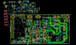
The layout of the main boards is done and it fits to 100mmx50mm including all options and just few SMD 1206.
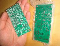
Itead delivered a bunch of 20 PCBs within one week. Few days processing at Itead + few days shipping. That's fast!
Seems like they made nice boards - hoping that there are no catastrophic errors from my side...
There will be pretty some time gap until the board is populated and tested, because I still have to order components and work is going to be very busy next month.
However I went on with my considerations on the optional gain board and
will post details soon.
Attachments
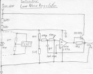
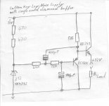
Low Noise Regulators for the Gain Board
The gain board is intended to become an universal input gain stage with optional limiter function and optional offset adjustment.
This gain board should be usable for any amplifier which needs an input gain stage and/or limiter.
The fundamental circuitry will be an instrumentation amplifier using a dual OP amp. The instrumentation amplifier with three OP amps did not make the race simply because of limited PCB size and current consumption.
Current consumption becomes a thermal concern when the supply of the OP amps is derived from the main rails through an onboard linear regulator.
For the gain control of the limiter I intend to use a vactrol (LDR+LED).
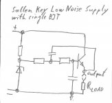
Some years ago I digged into solutions to achieve lowest noise supply rails.
The nicest solution was to use an active power sallen key filter.
Attached three possible implementations.
In the first implementation the resulting rail noise is dominated by the OP amp.
With slightly reduced impedances and 1/2 of a NE5532 the rail noise was around 5n/sqrt(Hz) - means the rail was by far cleaner than most audio signals.
For the gain board of the lite amp I intend to use a variation like in the third picture - let's see how far we can get with this simple solution.
The gain board is intended to become an universal input gain stage with optional limiter function and optional offset adjustment.
This gain board should be usable for any amplifier which needs an input gain stage and/or limiter.
The fundamental circuitry will be an instrumentation amplifier using a dual OP amp. The instrumentation amplifier with three OP amps did not make the race simply because of limited PCB size and current consumption.
Current consumption becomes a thermal concern when the supply of the OP amps is derived from the main rails through an onboard linear regulator.
For the gain control of the limiter I intend to use a vactrol (LDR+LED).
Some years ago I digged into solutions to achieve lowest noise supply rails.
The nicest solution was to use an active power sallen key filter.
Attached three possible implementations.
In the first implementation the resulting rail noise is dominated by the OP amp.
With slightly reduced impedances and 1/2 of a NE5532 the rail noise was around 5n/sqrt(Hz) - means the rail was by far cleaner than most audio signals.
For the gain board of the lite amp I intend to use a variation like in the third picture - let's see how far we can get with this simple solution.
Attachments
I've seen the right DC supply filter before and it works just fine.
About the DC/DC SMPS's, Recoms are definitely the best of their kind, but any DC/DC is a severe EMI source. Although the efficiency is tempting, I wouldn't use them anywhere near an audio signal. I know, class D is also a kind of SMPS, but DC/DC's are inherently worse because of their isolated grounds on input and output, those make nice dipole antennae.
Cheers, Marc
- Home
- Amplifiers
- Class D
- SystemD LiteAmp