Does anyone know the internal design of the LM723 ? How about the bandwidth etc of the internal error amp ? I'd like to try Jung's super-reg but I'm wondering how to connect a current source into the output of the error amp to bias into classA, and also a diode to control flow into its output. Here is the functional diagram :
Can I use the frequency compensation pin ? The diagram appears to suggest I can but of course I don't know what the actual circuit is.
I'm planning to connect the unregulated input supply directly to pin11, and a regulated supply to pin12. Vref connects to the non-inverting input via a low-pass filter.
I'll start with unity gain with the output connecting to the inverting input via a 10K resistor.
I was wondering if I could also use the zener between pins 9 and 10 as the zener on the output of the error amp ?
Any help is greatly appreciated !
An externally hosted image should be here but it was not working when we last tested it.
Can I use the frequency compensation pin ? The diagram appears to suggest I can but of course I don't know what the actual circuit is.
I'm planning to connect the unregulated input supply directly to pin11, and a regulated supply to pin12. Vref connects to the non-inverting input via a low-pass filter.
I'll start with unity gain with the output connecting to the inverting input via a 10K resistor.
I was wondering if I could also use the zener between pins 9 and 10 as the zener on the output of the error amp ?
Any help is greatly appreciated !
Last edited:

.SUBCKT LM723 2 3 4 5 6 7 9 10 11 12 13
* CL CS IN- IN+ VREF VCC- VZ OUT VC VCC+ FRCO
*
AZ1 15 12 ZENER1
J1 15 7 7 JMOD
R1 15 16 15K
Q1 16 16 17 QP1
Q2 20 16 19 QP1
Q3 20 21 7 QN1
C1 20 21 5PF
Q4 12 20 22 QN1
Q5 12 22 23 QN1
R2 23 6 100
AZ2 25 6 ZENER1
R3 21 25 30K
R4 25 7 5K
R5 12 17 500
R6 12 19 25K
R7 12 26 1K
Q6 27 16 26 QP1
Q7 23 27 28 QN1
Q8 27 28 29 QN1
R8 29 7 300
R9 28 7 20K
R10 12 30 1K
Q9 13 16 30 QP1
Q10 22 5 33 QN1
Q11 13 4 33 QN1
Q12 33 28 34 QN1
R11 34 7 150
Q13 12 13 36 QN1
Q14 11 36 10 QOUT
AZ3 10 9 ZENER2
Q15 13 2 3 QN1
R12 36 37 15K
I1 0 9 0
I2 0 2 0
I3 0 3 0
.MODEL QN1 NPN (BF=200 BR=2 RB=200 RC=200 RE=2 TF=0.35N IS=1E-14 VAF=125
+ CJE=1.0P VJE=0.7 MJE=0.33 CJC=0.3P
+ VJC=0.55 MJC=0.5 CJS=3.0P VJS=0.52 MJS=0.5 )
.MODEL QP1 PNP (BF=50 BR=4 RB=300 RC=100 RE=10 TF=30N IS=1E-14 VAF=50
+ CJE=0.3P VJE=0.55 MJE=0.5 CJC=1.0P
+ VJC=0.55 MJC=0.5 CJS=3.0P VJS=0.52 MJS=0.5 )
.MODEL QOUT NPN BF=80 RB=10 RC=5 IS=1E-16 VAF=50 CJE=10P CJC=10P
+ TF=3N TR=20N
.MODEL JMOD NJF VTO=-3 RS=1 RD=1 LAMBDA=.02 CGS=5P
.MODEL ZENER1 zener( v_breakdown=6.6 i_breakdown=0.02 r_breakdown=1.5 i_rev=1e-4 i_sat=1e-12)
.MODEL ZENER2 zener( v_breakdown=6.2 i_breakdown=0.02 r_breakdown=1.5 i_rev=1e-4 i_sat=1e-12)
.ENDS
Hi,
I have LT Spice but I don't know how to load code into it - sim noob. I saw a discussion about that code here :
lm723 ripple rejection ratio @100kHz
and it seems it has a very good ripple rejection and low noise, which is what i want - it'll be a pre-regulator feeding a 5V LT1763, a 2.8V LT1761 and a 5V LT1761, drawing 50mA in total (for the analogue supply of an AD1955 DAC).
 so I'm abandoning my efforts.
 Instead I'll use a jfet cascode to turn on an LM329 + red LED for 8.7V, and feed that via a low pass filter into the base of a BC550C.
ALWSR boards
Has anyone purchased and built any superreg boards from http://www.at-tunes.co.uk recently? These are the original Andrew Weekes design although I am unsure if he has anything to do with them now. I thought they originally were 2oz copper and now they are 1oz, other than that they are the same board I believe WJ indicated worked well. I want to build some +/- 15V for a low distortion oscillator using the AD825 and LM329 as per his boards so if anyone has built these what did you think of them?
Has anyone purchased and built any superreg boards from http://www.at-tunes.co.uk recently? These are the original Andrew Weekes design although I am unsure if he has anything to do with them now. I thought they originally were 2oz copper and now they are 1oz, other than that they are the same board I believe WJ indicated worked well. I want to build some +/- 15V for a low distortion oscillator using the AD825 and LM329 as per his boards so if anyone has built these what did you think of them?
DN2540 current source (not pre-regulator)
Not sure just what you mean here, Jack. The DN2540 cascode circuit referenced in the AX interview is operated as a current source, not a pre-reg as are featured in the vintage 2000 series type voltage regulators. The use of a current source feed (see 2009 article) is appropriate for use in a shunt regulator, i.e., the context of the interview discussion, and Fig. 1.
Hope this helps to clarify things.
ALWSR -- you should probably consider using the depletion MOSFET pre-regulator which WJ shows on his blog -- lower Zout than the Weekes version.
Not sure just what you mean here, Jack. The DN2540 cascode circuit referenced in the AX interview is operated as a current source, not a pre-reg as are featured in the vintage 2000 series type voltage regulators. The use of a current source feed (see 2009 article) is appropriate for use in a shunt regulator, i.e., the context of the interview discussion, and Fig. 1.
Hope this helps to clarify things.
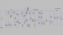
This is Russian answer to Jung super regulator, see circuit.
.
Output voltage is +15 Volts (positive).
Limit current is about 900mA - 1A .
.
Negative polarity, please, change transistors as follows.
NPN to PNP D44H11 to D45H11, 2N3904 to 2N3906
PNP to NPN D45H11 to D44H11, 2N3906 to 2N3904
Change diods to other polarity on circut.
Negative suply of OpAmp to output line of negative reg.
.
You may add LM317 (LM337) in input line as preregulator to this reg.
.
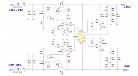
Prototype of this reg is circuit picture two.
.
Output voltage is +15 Volts (positive).
Limit current is about 900mA - 1A .
.
Negative polarity, please, change transistors as follows.
NPN to PNP D44H11 to D45H11, 2N3904 to 2N3906
PNP to NPN D45H11 to D44H11, 2N3906 to 2N3904
Change diods to other polarity on circut.
Negative suply of OpAmp to output line of negative reg.
.
You may add LM317 (LM337) in input line as preregulator to this reg.
.
Prototype of this reg is circuit picture two.
Attachments
Last edited:
In simulator LTSpice IV OpAmp NE5532 works better than OpAmp AD825.
Jenyok, what do you mean by 'works better'?
jan
We did this reg in two hard copy.
.
I mean better... So...
For example, simulate our Russian circuit and Jung super reg circuit in LTSpice or other simulate program and see result of simulation.
And...
You will see, that our Russian circut is more better then Jung reg circuit.
In our Russian circuit is smaller instability of voltage output under loading output.
In our Russian circuit pulsation of voltage output is smaller than in Jung reg circuit.
In our Russian circuit coefficient stabilizing of output voltage is more than 70000 (> 100dB), in Jung reg circuit coefficient stabilizing of output voltage is less than 70000 .
And so on...
Last edited:
- Status
- This old topic is closed. If you want to reopen this topic, contact a moderator using the "Report Post" button.
- Home
- Amplifiers
- Power Supplies
- Super Regulator, collecting the facts