I can't find the schematic but it looks like the base ties to the output through 4R7 resistors?
..... I think it's ok ,just see partial schematic attached below
")
Alex
Attachments
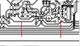
Alex,..... PCB ready , please someone check if it's correct layout . I will post in B&W the layout of PCB .
Schematic will follow soon .
Regards ,Alex
a much better layout.
The V+, V- and Power Ground enter the PCB in a tight close coupled group. This minimises Loop Area and thus minimises interference.
Output is also fairly close to this Power Group again minimising Loop Area.
Well Done.!
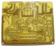
Here is the original PCB.Please check...
An externally hosted image should be here but it was not working when we last tested it.
..... PCB ready , please someone check if it's correct layout . I will post in B&W the layout of PCB .
Schematic will follow soon .
Regards ,Alex
Hello Alex don't get upset with me but for manufacturing PCB's will be no problem at all but for etching diy those traces are I think way too close each other maybe you can give a few extra millimeters so etching will be no problem.
Regards
Juan
Attachments
Dear Alex? proper installation of the diagram is always running and I have not changed anything on the same pcb mount components so the dc leakage....yes of course , why not , here in attachment are all files for toner transfer metod
Regards ,Alex
An externally hosted image should be here but it was not working when we last tested it.
Hi All,
Please check it if any error
...I like the dual pot arrangement.
Works for both a lay flat skeleton pot and for an inline multi-turn pot.
Well done.
What about adding an offset pin for the staggered pin multi turn pot.
Add dual or multi pin pitch options for all your capacitors.
If possible orient all your electros in the same direction.
Works for both a lay flat skeleton pot and for an inline multi-turn pot.
Well done.
What about adding an offset pin for the staggered pin multi turn pot.
Add dual or multi pin pitch options for all your capacitors.
If possible orient all your electros in the same direction.
Thanks AndrewT for your suggestionI like the dual pot arrangement.
Works for both a lay flat skeleton pot and for an inline multi-turn pot.
Well done.
What about adding an offset pin for the staggered pin multi turn pot.
Add dual or multi pin pitch options for all your capacitors.
If possible orient all your electros in the same direction.
I will add some pad latter
all the electrolyte are at same direction
Right now I already make a board to test it, I hope no oscillation or other unwanted one...
I will share the layout after it is "tested OK"
Hi Vostro, I will check that out after I finish stuffing itHi John, do the mje340/350 inthe middle of pcb need heatsinks, so do they run cool enough on the lower supply voltage
(one PCB already done)
I will add a little heatsink for each transistor (I don't know if it is need or not)
Regards
Attachments
Last edited:
Thanks AndrewT for your suggestion
I will add some pad latter
all the electrolyte are at same direction
Right now I already make a board to test it, I hope no oscillation or other unwanted one...
I will share the layout after it is "tested OK"
Hi Vostro, I will check that out after I finish stuffing it
(one PCB already done)
I will add a little heatsink for each transistor (I don't know if it is need or not)
Regards
Nice pcb,
Regards
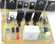
Ok, it tested OK
Dear sir Mile,
thanks for your SR100
this PCB already tested...
PCB size is : 95 * 80 mm
I need to make another channel
the MJE's need small heatsink & only a little warm
Warm Regards
Dear sir Mile,
thanks for your SR100
this PCB already tested...
PCB size is : 95 * 80 mm
I need to make another channel
the MJE's need small heatsink & only a little warm
Warm Regards
Attachments
Dear sir Mile,
thanks for your SR100
this PCB already tested...
PCB size is : 95 * 80 mm
I need to make another channel
the MJE's need small heatsink & only a little warm
Warm Regards
Nice work, thanks for this pcb design,
Regards
who can tell me a software for pcb's please.
I use multisim software for schematics and he have ultrasim for PCB but it's look very strange...
Hi, DipTrace - Schematic and PCB Design Software as an option...
Cheers,
Valery
Thank You Vzichenko !
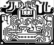
B&W PCB
Any progress ?..... PCB ready , please someone check if it's correct layout . I will post in B&W the layout of PCB .
Schematic will follow soon .
Regards ,Alex
Now i work at another amplifier but the next one will be SR800Any progress ?
I will come with new when i star to build him!
- Home
- Amplifiers
- Solid State
- Studio Reference Amplifier