symmetry
Interesting design, Jonathan.
If R5=R6=R7=R8=Rc and R3=R4=Re, then the vas stage differential current will be proportional to Va+Vb-2.Vout.(R22/(R21+R22)).Rc/Re
I believe there may be a simple connection error because as drawn the vas stages appear to be fighting with each other.
Interesting design, Jonathan.
If R5=R6=R7=R8=Rc and R3=R4=Re, then the vas stage differential current will be proportional to Va+Vb-2.Vout.(R22/(R21+R22)).Rc/Re
I believe there may be a simple connection error because as drawn the vas stages appear to be fighting with each other.
Traderbam:
The schematic was adopted from Onkyo's promotional literature. There _is_ more stuff in the schematic, like a BJT cascode for the second-stage, an extra follower-type predriver hanging off the second stage (before the Bi-MOS section), while the output stage consists of three PP pairs. OTOH, I didn't think that these were required to envision and understand the basic operation of this circuit.
BTW, re the input stage, I know of someone who built a circuit using something like it. I recall that he mentioned that the CMRR was extremely high, but OTOH, the thermal DC stability was rather poor (temperature-induced Vbe shifts?).
regards, jonathan carr
The JFET/BJT Rush cascode
I realize I was making a mistake in my thinking yesterday. For
some "mysterious" reason I managed to convince myself that
the Vbe's of two BJTs in a Rush cascode would add up to zero,
so the bases are at the same voltage at the Q point. That is
of course absolutely wrong, so I think Halo might have been
right in his suggestion on the use of the JFET. Two BJTs
cannot cancel out, while a JFET and a BJT or two JFETS can.
Still, using two JFETs would have seemed more reasonable,
so the mystery is not completely solved. I don't know what
type of JFET was used, so maybe it has a reasonably low
Id at Vgs around 0.6V. Still, two complementary JFETs would
match up better, but perhaps it was difficult to find a suitable
pair 20 years ago?? I have been thinking also of an alternative
explanation. Maybe the purpose of the BJT is to get a
low-impedance input so it is actually some kind of current
feedback? I am not sure if a Rush cascode would have a low
input impedance, though.
Fred Dieckmann notified me that some of the component values in my original schematic were just too far out to be usable - like putting a decimal point on the wrong location. :-(
Here is a slightly cleaned-up schematic with what I hope are more appropriate component values. In the interest of staying with easily found parts, I replaced the current sources with resistors. But if you have access to a variety of constant-current devices, or are willing to roll your own CC circuit, the current sink under the input differential should be 6.4mA, while the current source feeding the second-stage should total 32.7mA.
BTW, my interest in the current thread lies in the use of global NFB through the emitters of the input devices. More specifically, being able to set one path for the input signal and a separate path for the feedback, without adding to the total device count. At this stage, I mainly want to understand fully how this method works. How the idea is applied, for example, non-inverting operation, inverting, feedback to the same side, feedback to the opposite side etc. is a topic of interest to be sure, but one for another day. Apologies if my initial comment about inverting-mode circuits was misleading to anyone.
regards, jonathan carr
Attachments
jcarr said:BTW, my interest in the current thread lies in the use of global NFB through the emitters of the input devices.
Jonathan, I recall that this type of feedback was also used by
James Bongiorno in his Ampzilla III, a fully balanced bridge
amplifier from the early 1980s. If you are interested, there is
more info and a schematic at:
http://home.kimo.com.tw/skychutw/ampzilla/AmpzillaIII.htm
Re: The JFET/BJT Rush cascode
and some lower resistors as feedback path.
I think one of the reasons for using this technique
is to have an amp with higher speed.
I think AKSA mentioned this in comments on jcarr's circuit.
And at higher speeds lower resistors/more current behave better.
Due to capacitance getting noticable in metalfilm resistors.
------------------
I had a look at what JFETs could be good with a small signal BJT.
As our selections, within Sewden, are almost only what www.elfa.se
can provide, I only found BF245B to match, if I remember correctly.
But BF245A & BF245B is for low noise at HF, high freq.
Aimed for use in radio-technique.
But it could be worth a try.
Good with JFET BF245 is that they are very commonly available everywhere.
Lower price also, compared to Audio JFETs.
/halo - Best? - Yes!! Chess-player at www.diyaudio.com
It can very well be so, that it is better using BJTChrister said:---------------
I don't know what
type of JFET was used, so maybe it has a reasonably low
Id at Vgs around 0.6V. Still, two complementary JFETs would
match up better, but perhaps it was difficult to find a suitable
pair 20 years ago?? I have been thinking also of an alternative
explanation. Maybe the purpose of the BJT is to get a
low-impedance input so it is actually some kind of current
feedback? I am not sure if a Rush cascode would have a low
input impedance, though.
and some lower resistors as feedback path.
I think one of the reasons for using this technique
is to have an amp with higher speed.
I think AKSA mentioned this in comments on jcarr's circuit.
And at higher speeds lower resistors/more current behave better.
Due to capacitance getting noticable in metalfilm resistors.
------------------
I had a look at what JFETs could be good with a small signal BJT.
As our selections, within Sewden, are almost only what www.elfa.se
can provide, I only found BF245B to match, if I remember correctly.
But BF245A & BF245B is for low noise at HF, high freq.
Aimed for use in radio-technique.
But it could be worth a try.
Good with JFET BF245 is that they are very commonly available everywhere.
Lower price also, compared to Audio JFETs.
/halo -
Best? - Yes!! Chess-player at www.diyaudio.com >Primare also take feedback to the emmiters of the differential, in some of their amps.<
Jam, you may be right. I also seem to recall having heard something about Primare using the emitters of the differentials for global NFB. Can you sketch out any sort of schematic, or do you recall any comments about the goals and characteristics of this type of circuit?
>I would like to know that if you apply feedback in this way do you gain any advantages in speed or distortion characteristics?<
I would like to know, too. Going into the emitters certainly would encourage the use of low-impedance NFB networks, which would be an asset for speed. For non-inverting operation, low-impedance NFB networks are fine, but when you go to inverting configurations, the impedance of the NFB network nearly always has to be set on the high side to prevent loading down the source component too much. Another way is to add an input buffer specifically to drive the low-impedance shunt NFB network, but that means more semiconductor junctions, and more complexity overall.
With the emitter NFB approach, the input devices act as normal voltage amplifiers for signals entering through their bases, but for the NFB signals that enter through their emitters, the input devices probably function as cascodes. I figure that integrating the emitter NFB idea into a real inverting-polarity configuration may lead to the ability to use a low-impedance shunt feedback network without imposing any sort of tough load on the source component.
>I got issue 21 of Hi Fi + today. They really like your preamp, one day I hope you release the design.<
Well, I continue to work on it, and it continues to improve. But it is quite complex. The amplification topology is relatively complex, and there are 12 discrete-device voltage regulators per amplifier module. Partly because there is so much circuitry, I have gone to stacked dual 4-layer boards combined with p2p "air-dielectric" circuitry for critical amplification nodes. If any design were released in the future, it would _have_ to be very much simplified from what it is right now - otherwise it would most likely be unbuildable.
And in my upcoming "3.1" design, I intend to use a triple 4-layer board sandwich. Simplicity just doesn't appear to be one of my virtues....
regards, jonathan carr
Jam, you may be right. I also seem to recall having heard something about Primare using the emitters of the differentials for global NFB. Can you sketch out any sort of schematic, or do you recall any comments about the goals and characteristics of this type of circuit?
>I would like to know that if you apply feedback in this way do you gain any advantages in speed or distortion characteristics?<
I would like to know, too.
Going into the emitters certainly would encourage the use of low-impedance NFB networks, which would be an asset for speed. For non-inverting operation, low-impedance NFB networks are fine, but when you go to inverting configurations, the impedance of the NFB network nearly always has to be set on the high side to prevent loading down the source component too much. Another way is to add an input buffer specifically to drive the low-impedance shunt NFB network, but that means more semiconductor junctions, and more complexity overall.With the emitter NFB approach, the input devices act as normal voltage amplifiers for signals entering through their bases, but for the NFB signals that enter through their emitters, the input devices probably function as cascodes. I figure that integrating the emitter NFB idea into a real inverting-polarity configuration may lead to the ability to use a low-impedance shunt feedback network without imposing any sort of tough load on the source component.
>I got issue 21 of Hi Fi + today. They really like your preamp, one day I hope you release the design.<
Well, I continue to work on it, and it continues to improve.
But it is quite complex. The amplification topology is relatively complex, and there are 12 discrete-device voltage regulators per amplifier module. Partly because there is so much circuitry, I have gone to stacked dual 4-layer boards combined with p2p "air-dielectric" circuitry for critical amplification nodes. If any design were released in the future, it would _have_ to be very much simplified from what it is right now - otherwise it would most likely be unbuildable.And in my upcoming "3.1" design, I intend to use a triple 4-layer board sandwich. Simplicity just doesn't appear to be one of my virtues....
regards, jonathan carr
"I have been thinking also of an alternative
explanation. Maybe the purpose of the BJT is to get a
low-impedance input so it is actually some kind of current
feedback?"
My problem is that I cannot see the difference between an npn-pnp LTP and an npn-npn LTP. Both have the same input Z on both inputs - both through two emitters. So why use this topology rather than a standard LTP?
Even surmising that if you are going to use a JFET input that to have a low Z on the feedback input you need to use a bipolar. But that doesn't figure either since the Z will be a function of the JFET in series with the BJT, not just the BJT.
All I can think is saving parts or some CMRR/PSRR benefit.
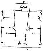
This is a very interesting circuit, Jonathan, with strong aesthetic value. I have taken the liberty of sketching a simpler version of the same topology (hopefully) below, as an aid to wrapping our minds around it.
I look at it this way: If you split it down the middle, you get two mirror image gain stages, both single-ended "current feedback" types. By their symmetric nature, the junction between the two Emitter resistors on the first differential (input) pair and the Emitter resistors on the second differential pair will be at virtual AC ground for the case of an ideal circuit.
When we remove the idealness we note that non-common mode distortion/noise originating in one side appears at the Emitters of the differential pair, creating negative feedback for the side in question, but generating the same distortion on the other side in an additive way. However, at the same time we see that this additive distortion tends to be rejected by the differential connection of the emitters of the second gain stage. But this rejection also tends to inhibit feedback correction in the side originating the distortion.
You can see these effects by taking a copy of the schematic and introducing a "positive glitch" at the output of one half and then following through the whole circuit, noting amplification and changes in polarity as it passes through each part of the circuit. (This is how I spent years evaluating candidates for SuperSymmetry)
So where does that leave us? The performance will be very sensitive to the balance of values of the four feedback resistors in the input stage, and you may have to introduce some lossiness to the current source I1 or even just replace it with a resistor to get what you want.
Very suitable subject for DIYers to experiment with.
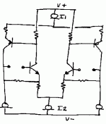
Nelson diagram and text in short
First I thought Nelson had published a new
Car-Amplifier.
To please some billions of Car-Audio Entusiasts in this World of highways.
But that will be a future possibility.
-----------------------------------------------
I am not the only one gettin' on the roll by this circuit, I see.
Here is the principal diagram of Nelson's.
For to simplify the understanding.
/halo
- carramp.bmp -Nelson Pass said:This is a very interesting circuit, Jonathan, with strong aesthetic value. I have taken the liberty of sketching a simpler version of the same topology (hopefully) below, as an aid to wrapping our minds around it.
-------------------------------------------------------------------
Very suitable subject for DIYers to experiment with.
First I thought Nelson had published a new
Car-Amplifier.
To please some billions of Car-Audio Entusiasts in this World of highways.
But that will be a future possibility.
-----------------------------------------------
I am not the only one gettin' on the roll by this circuit, I see.
Here is the principal diagram of Nelson's.
For to simplify the understanding.
/halo
Attachments
jcarr - EmitterNFB BTL-amp - version 2
with some alterations inspired by Fred Dieckmann
jcarr - EmitterNFB BTL-amp - version 2 (revised)jcarr said:Fred Dieckmann notified me that some of the component values in my original schematic were just too far out to be usable - like putting a decimal point on the wrong location. :-(
Here is a slightly cleaned-up schematic with what I hope are more appropriate component values. In the interest of staying with easily found parts, I replaced the current sources with resistors. But if you have access to a variety of constant-current devices, or are willing to roll your own CC circuit, the current sink under the input differential should be 6.4mA, while the current source feeding the second-stage should total 32.7mA.
BTW, my interest in the current thread lies in the use of global NFB through the emitters of the input devices. More specifically, being able to set one path for the input signal and a separate path for the feedback, without adding to the total device count. At this stage, I mainly want to understand fully how this method works. How the idea is applied, for example, non-inverting operation, inverting, feedback to the same side, feedback to the opposite side etc. is a topic of interest to be sure, but one for another day. Apologies if my initial comment about inverting-mode circuits was misleading to anyone.
regards, jonathan carr
with some alterations inspired by Fred Dieckmann
Attachments
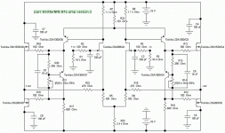
I see that Fred has anticipated some of my thoughts and has addressed them.
This newer version will have a couple of things we want to pay attention to: It will want a balanced source for sure, and it will need a regulated supply, as our PSRR has declined with the replacement of the negative side current source with a resistor. It might be reasonable to reinstate the current source in this spot. Also, I would be inclined to put back some Emitter resistance on the PNP transistors.
This newer version will have a couple of things we want to pay attention to: It will want a balanced source for sure, and it will need a regulated supply, as our PSRR has declined with the replacement of the negative side current source with a resistor. It might be reasonable to reinstate the current source in this spot. Also, I would be inclined to put back some Emitter resistance on the PNP transistors.
Re: Nelson diagram and text in short
Hmmm, I don't know if any of these are still in that business....

pass/ - maybe you don't want him designing your car audio anyway.
Actually it belongs more to the past. I have designed car audio for Soundstream, Linear Power, Adcom and another company in Thailand.halojoy said:First I thought Nelson had published a new
Car-Amplifier.
To please some billions of Car-Audio Entusiasts in this World of highways. But that will be a future possibility.
Hmmm, I don't know if any of these are still in that business....
pass/ - maybe you don't want him designing your car audio anyway.
Re: Re: Nelson diagram and text in short
Adcom appears to be out of the car audio bidness. Linear's still at it and Soundstream is still in business but under new ownership. Was talking to the folks over at R Squared a few years back and they said Stewart just up and disappeared. Dunno what happened after that.
By the way, Lorin still has that monster regulated 12 volt power supply he built for bench testing the old Soundstream stuff.
se
Nelson Pass said:
Actually it belongs more to the past. I have designed car audio for Soundstream, Linear Power, Adcom and another company in Thailand.
Hmmm, I don't know if any of these are still in that business....
Adcom appears to be out of the car audio bidness. Linear's still at it and Soundstream is still in business but under new ownership. Was talking to the folks over at R Squared a few years back and they said Stewart just up and disappeared. Dunno what happened after that.
By the way, Lorin still has that monster regulated 12 volt power supply he built for bench testing the old Soundstream stuff.
se
Dear Nelson:
Your simplified circuit is conceptually spot-on.
BTW, the schematics that I have drawn up have been partly triggered by your "Monolithic SuperSymmetry" post. I liked the conceptual ideas, but I didn't like the high impedances that usually accompany shunt feedback schemes (unless you are dealing with low-impedance source components like moving-coil cartridges).
With the emitter NFB circuit, I wanted to propose an alternative feedback method that would allow the impedance of the NFB network to be reduced substantially without loading down the source component. It isn't an "X" or Monolithic SuperSymmetry circuit yet, but I think that this can be done. And in the spirit of the X and SuperSymmetry circuits, it felt proper to keep the circuit itself fully symmetrical - and simple.
So if someone wants to try to incorporate the emitter NFB idea into one of the "X" circuits or the Monolithic SuperSymmetry, that would be great!
>You get two mirror image gain stages. By their symmetric nature, the junction between the two Emitter resistors on the first differential pair and the second differential pair will be at virtual AC ground.<
And ideally those junctions should be very high impedance.
>non-common mode distortion/noise originating in one side appears at the Emitters of the differential pair, creating negative feedback for the side in question, but generating the same distortion on the other side in an additive way. However, this additive distortion tends to be rejected by the differential connection of the emitters of the second gain stage.<
Yes.
>But this rejection also tends to inhibit feedback correction in the side originating the distortion.<
Valid point, and one that I don't have a solution for (yet).
>The performance will be very sensitive to the balance of values of the four feedback resistors in the input stage.<
Agreed.
>you may have to introduce some lossiness to the current source I1 or even just replace it with a resistor to get what you want.<
My preference would be to keep it a current source. The revised schematic that I posted has resistors instead of current sources, but this is mainly because I was thinking of people who may possibly want to build the circuit instead of just think about it, and don't have ready access to current sources. If I build this circuit for myself, it will be with current sources instead of resistors.
>Very suitable subject for DIYers to experiment with.<
I hope so, and also one that I hope will be combined with other ideas.
best, jonathan carr
As I have implied, these were issues I wrestled with for many years in the X development, and it is familiar territory.
By the way, you will note that the XA amps, and the Aleph X schematics on that thread incorporate Source feedback in a similar manner, but it is used only for common mode errors, ie absolute DC offset. This is done by reducing the values of
the Source resistances (in your case the 100 ohms) to 0.
By the way, you will note that the XA amps, and the Aleph X schematics on that thread incorporate Source feedback in a similar manner, but it is used only for common mode errors, ie absolute DC offset. This is done by reducing the values of
the Source resistances (in your case the 100 ohms) to 0.
Balanced feedback folded-cascode
Today I stumbled across a webpage discussing circuitry concepts that are fairly similar to some things I have been intermittently experimenting with for some time.
http://home.kimo.com.tw/skychutw/DIY/Audio/Siraya/index.htm
The website homepage:
http://home.kimo.com.tw/skychutw/
I will caution that the similarities are in the overall thinking rather than in the details of the actual circuits. In fact, I would most likely _not_ build Figure 5 nor Figure 6 without revising them.
regards, jonathan carr
- Status
- This old topic is closed. If you want to reopen this topic, contact a moderator using the "Report Post" button.
- Home
- Amplifiers
- Solid State
- Source/emitter global NFB amp