My regulated power supply has convenient voltage and current meters built in.
Lacking that, a low value Drain resistor would work fine.

ya see
whenever I get smart , he sez otherwise


Sony VFET rank is just the last digit. For J18/K60 it is defined as Vgs needed for Id=100mA @ Vds=50V, ONLY for ranks 3 to 8, and is approx. 7.5+(2.5 x rank) volts.
There are also rank 1 and 2, which do not correspond to these specs, they have lower Idss and often higher mu.
The ranking scheme should be the same for J28/K82. Most J28/K82 are two-chip devices, but the chips are NOT equal to J18/K60 even though they are almost exactly the same size. J28/K82 input capacitance is lower, mu is twice that of J18/K60. There are (but they are VERY rare) original J28/K82 with a single larger chip. This is the original design described in Sony's AES papers on the VFET. It was originally intended for analog amplification, and later optimized for their class D amp (TA-N88). The difference is that to my knowledge all the ones in the N88 amp are rank 3, whereas the original ones had ranks 3 to 8 just like J18/K60 - BUT read below re Chinese fakes.
A curve tracer will show that there is a lot of variation even within the same rank. Pairing for direct parallel operation whould be done at least at two points. For many in parallel, the differences will even out.
Tempco of all Sony VFETs is slightly negative.
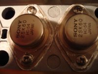
Chinese parts: BUYER BEWARE!!! The newest fad is to sell you exactly what you want, by stripping the original markings and stamping (or most likely inkjet-printing) the ones you wanted. Becasue VFETs are easy to check for, you will likely get VFETs but not the rank and oftennot even the type you think you got. Usually it's J18/K60, rank 1 or 2, relabelled. China sourced K82 are currently all re-labelled K60, rank 1 or 2.
There are also rank 1 and 2, which do not correspond to these specs, they have lower Idss and often higher mu.
The ranking scheme should be the same for J28/K82. Most J28/K82 are two-chip devices, but the chips are NOT equal to J18/K60 even though they are almost exactly the same size. J28/K82 input capacitance is lower, mu is twice that of J18/K60. There are (but they are VERY rare) original J28/K82 with a single larger chip. This is the original design described in Sony's AES papers on the VFET. It was originally intended for analog amplification, and later optimized for their class D amp (TA-N88). The difference is that to my knowledge all the ones in the N88 amp are rank 3, whereas the original ones had ranks 3 to 8 just like J18/K60 - BUT read below re Chinese fakes.
A curve tracer will show that there is a lot of variation even within the same rank. Pairing for direct parallel operation whould be done at least at two points. For many in parallel, the differences will even out.
Tempco of all Sony VFETs is slightly negative.
Chinese parts: BUYER BEWARE!!! The newest fad is to sell you exactly what you want, by stripping the original markings and stamping (or most likely inkjet-printing) the ones you wanted. Becasue VFETs are easy to check for, you will likely get VFETs but not the rank and oftennot even the type you think you got. Usually it's J18/K60, rank 1 or 2, relabelled. China sourced K82 are currently all re-labelled K60, rank 1 or 2.
Sony VFET rank is just the last digit. For J18/K60 it is defined as Vgs needed
for Id=100mA @ Vds=50V, ONLY for ranks 3 to 8, and is approx. 7.5+(2.5 x rank) volts.
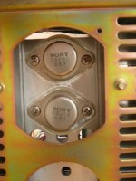
Thanks for the detailed information. The 2SK82 and 2SJ28 that I obtained
from circuitdiy.com are labeled as KE33. They also have some inventory of
KF33 for the 2SJ28.
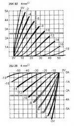
I did not perform tests at 100mA and 50V as this spot is not close to my
intended use. I tested for Vgs at 20V Vds at 0.5A and 1.0A Ids.
The result is that all the parts conform roughly to the attached curve trace,
the average being around 8V Vgs at 1 amp for the 2SK82 and 10V for the
2SJ28. There is a decent population of parts near the average so that it is
not difficult to get matches, but you will see parts spread out by a volt or
so. Under these conditions, a difference of 1 volt Vgs would mean about
0.5A (about 50mA for each 0.1 difference).
If you are matching for parallel operation at these sorts of Class A currents
I recommend matching the parts, to 0.1V if feasible and 0.2V would be an
acceptable figure. If you are using these parts in parallel, get some extras.
If not, no worry (but test them anyway).
Attachments
Thanks for the detailed information. The 2SK82 and 2SJ28 that I obtained
from circuitdiy.com are labeled as KE33. They also have some inventory of
KF33 for the 2SJ28.
I did not perform tests at 100mA and 50V as this spot is not close to my
intended use. I tested for Vgs at 20V Vds at 0.5A and 1.0A Ids.
The result is that all the parts conform roughly to the attached curve trace,
The published curves are for the 'old' single-die J28/K82 - I actually have a few and of different rank. Still, the 'new' 2-die ones were optimized old ones so the curves are roughly the same. The biggest differences occur at low Vds and high Id.
The device code (of which the last digit is the rank) for the single die ones starts with H, while available ones are usually J or K (so you can deduce the letters are in ascending order). It seems a small number of these single die ones were produced and should be treated as prototypes.
The reason the ranking system was defined as it was is because it is closest to quiescent conditions in Sony's first generation Vfet amps. The rank table can be found if one looks carefully at the service manual for the TAN8550 power amp.
Regarding the fads: are they really relabelling old VFETs to look like other old VFETs? J18/K60 relabelled to J28/K82. Fantastic, I believed it was more or less just any old TO3 that was relabelled. Is this caused by Nelson Pass' adventures with J28/K82 then?!
Yes, they are really genuine Sony VFETs (initially, of course, there was all sorts of fakery but since VFETs measure rather uniquely even by a simple DMM, this is rare these days, plus Sony used a slightly distinctive TO-3 style case).
In one case, I actually got recycled ones that had the nickel stripped off, the whole case was then re-tinned and new markings stamped on, so it's a uniform but dull silver color. And - amazingly - these are good genuine J18/K60. I've also had a mixed batch of J28/K82 that turned out to be single chip J28, double chip J28 and genuine K60 re-labelled as K82.
The most common 'fake' are re-labelled rank 1 and 2 devices. These have rather different characteristics and were never used in production, but there are indications that they were offered in their day to DIY-ers in Japan.
Other types were available as well, most notably Yamaha. However, these seem all to come from the same source, and about 25% of the P-ch parts don't work while only about 25% of the N-ch parts work. The rest are fried, probably by some 'genius' attempting to 'test' them on a curve tracer set up for BJTs. VFETs have a rather unique failure mode (they are actually incredibly robust) to do with positive G-S and gate current. When this is over spec, the VFET will deteriorate - the G-channel 'diode' breakdown voltage will reduce to a point where G-D breakdown will occur long before D-S breakdown, and also mu will lower and Idss will lower. It will still look like a triode on a tracer. If the gate current becomes very high very quickly, the pin to chip bond wire will go open like a fuse, while the actual chip will survive! This is the most common mode of failure in Sony gen. 1 VFET amps that still have functioning bias supplies. In any case all of the failed Yamaha parts that still had an intact bond to the chip had this tell-tale failure, which was probably the result of trying to drive the gate as if it were the base of a BJT.
BTW: not commonly known is that the VFET has a 'beta' area and indeed does appear to work as a BJT for positive Vgs, with current saturation and pentode-like curves! This mode is extremely useful for high speed switching, it reduces apparent Rdson by easily a factor of 10, but maximum Ig spec must be observed.
Last edited:
Thank you very much for this information. Very good.
It is also quite amazing that devices were made, but never used in commercial products, if I understand right, but only for the DIY community of the day.
I guess quite a lot of these devices must have been made also.
We can hope the Pass 40th Anniversary Commemorative VFET amplifier will give Sony a push towards making new VFETs - although don't hold your horses!
Driver for N-channel VFET output stage of power amplifier
US 5783970 A :
Patente US5783970 - Driver for N-channel VFET output stage of power amplifier - Patentes do Google
Have a nice day

US 5783970 A :
Patente US5783970 - Driver for N-channel VFET output stage of power amplifier - Patentes do Google
Have a nice day
Driver for N-channel VFET output stage of power amplifier
US 5783970 A :
Patente US5783970 - Driver for N-channel VFET output stage of power amplifier - Patentes do Google
Have a nice day
Check links before posting - VFET in this case referst o vertical MOSFETs, and has nothing to do with the topic of this thread.
There are several topologies especially suited for VFETs, like equivalents of SE triode amps - these are by definition class A.
However, class A push-pull is especially interesting with VFETs because they have a square law characteristic. One consequence is that it does not require biassing to half the load current to ensure voltage clipping will occur before either side goes into cut-off. A lower bias current is required, resulting in 'hyperbolic-like' operation, so you get the benefits of class a with substantially reduced heat generation.
However, class A push-pull is especially interesting with VFETs because they have a square law characteristic. One consequence is that it does not require biassing to half the load current to ensure voltage clipping will occur before either side goes into cut-off. A lower bias current is required, resulting in 'hyperbolic-like' operation, so you get the benefits of class a with substantially reduced heat generation.
However, class A push-pull is especially interesting
with VFETs
because they have a square law characteristic. One consequence is that it
does not require biasing to half the load current to ensure voltage clipping will
occur before either side goes into cut-off. A lower bias current is required,
resulting in 'hyperbolic-like' operation, so you get the benefits of class a with
substantially reduced heat generation.
Yes, something I took advantage of in the Common Drain Push Pull output
stage of the Sony Commemorative Amp, whose Class A output power is about
twice that of what you would "classically" expect. Actually, it's more than
that, but when the current in the "unused" devices becomes a low percentage
of the idle value, you start stretching the point.
...Class A output power is about
twice that of what you would "classically" expect. Actually, it's more than
that, but when the current in the "unused" devices becomes a low percentage
of the idle value, you start stretching the point.
Yes, this was used in the old Sony amps even in 'class AB' because the crossover region becomes very stretched and smooth.
The same concept is well known in tube OTL amps, where low mu trioder are used, which are actually quite non-linear and very difficult to drive into cut-off. If they were perfectly linear, the require idle current would be so high the dissipation would be way over the maximum. In reality, a fraction of it is needed, usually half or even less.
What is the difference in the E series and F series?
Regarding biasing and Q points?
KF is a newer batch than KE, they should have exactly the same spec - and the same tolerances! - since by that time the production process was set-up and it remained that way till the end. So far I have not been able to figure out if there were batches after KF, since it's likely that most of the parts remaining after production stopped went to various dealers and remained in storage for a long time, and with the latest fad of re-marking, it's likely they were re-marked with who knows what code.
Yes, this was used in the old Sony amps even in 'class AB' because the crossover region becomes very stretched and smooth.
The same concept is well known in tube OTL amps, where low mu triodes are used, which are actually quite non-linear and very difficult to drive into cut-off. If they were perfectly linear, the require idle current would be so high the dissipation would be way over the maximum. In reality, a fraction of it is needed, usually half or even less.
The concept was put to use in the Threshold "dynamic bias" series, where the
dissipation was about half the expected value, or roughly equal to the rated output.
As I mentioned, you can stretch that argument to say that an amplifier with
very low bias is still Class A just because there is still some conduction in
the unused half.
...you can stretch that argument to say that an amplifier with very low bias is still Class A just because there is still some conduction in the unused half.
Yes, but of course, it's the shape of the transfer function that ultimately decides how far you can stretch it
and for VFETs it's rather simple to get a substantial 'extra' by default, without any extra circuitry - so I'd count that as a plus - Status
- This old topic is closed. If you want to reopen this topic, contact a moderator using the "Report Post" button.
- Home
- Amplifiers
- Pass Labs
- Sony SITs - 2SK82 E Rank With 2SJ28 F Rank