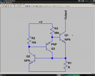
That is neat. It worries me though. The arrangement of Q1 and Q3 makes a discrete triac (diac? SCR? Don't remember...). This arrangement boosts gain because of having positive feedback. It is too easy for this to become negative impedance, and then oscillation. For instance there is this CCS below. It has incredibly high output impedance. In fact, it is negative output impedance. This is because of the discrete SCR, causing positive feedback. This CCS has a knack for oscillation.
If carefully controlled, I think the discrete SCR could have potential for a very simple but extreme gain stage. After all, it's usual use is as a latch because of it's super high gain (and positive feedback).
Have you seen the SPICE models at Cordellaudio.com? Cordell made them himself, I put them in my default library...
- keantoken
Attachments
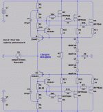
The object of R1 (schematic #583) is a constant current source across VBE Q3.
Resistor across VBE assures Q3 can be turned off anytime, if I wished it so.
Real SCR would not have external access to base of Q3, and can't be turned off.
R7 also assures Q1 could be turned off anytime, if I wished it so. I deleberately
do not allow anything to be turned off. But thats another story, not an SCR...
Your drawing #584 Q3 would latch like SCR as well, without R2 being there.
But you have neglected to use R2 as CCS to increase emitter impedance Q2.
10K? A much smaller resistor across Q3 VBE would slope like 100's of Kohms.
If looking too much like discrete SCR worries, return collector to the other side
of the Allison's voltage gap.
I have a newer version of drawing does exactly that. Plus some Schade from
collector to base of my Q1 (and its compliment) to linearize and nail down error
voltage gain, in the event some error is unfixable. Considerably more stable...
Last edited:
")
Sounds right to me. Did you notice that your arrangement is eerily similar to that CCS? Except in this case the bias voltage changes to produce output.
BTW, C2 is backwards.
- keantoken
"to that CCS", what ccs or post# we talking bout? You lost me.
----edit----
Oh, #584 "This CCS has a knack for oscillation.", I'm back on page...
I agree, nothing there to keep error voltage gain from going apesh.
Once an unfixable glitch happens, its completely lost its marbles.
Too little voltage on both collectors requires bases saturate, so
probably sluggish. Q2 collector idles at same voltage as its base.
Last edited:
In operation Vce changes very little, and Ic changes are in uA, so I don't think saturation is a big problem. If used in an analogue saw generator with fast enough pulses, a schottkey B-C will decrease recovery time, best to choose high current, low Cj. If you want to increase Vce you can put a diode at Q1's emitter, maybe an LED, or a shorted MOSFET. Or just a resistor to be boring.
In simulation the CCS doesn't show any latching or motorboating, although it does exhibit ringing and often legitimate oscillation.
In describing the CCS I neglected line rejection, which is different from output impedance. Line rejection for this CCS is unfortunately not high because R3 directly injects rail noise into the output current.
- keantoken
One day you will discover for yourself not to run BJT
collectors at or below base voltage in audio circuits.
Unless you have huge amounts of drive both directions,
or speed does not matter.
Even worse in MOSFETs for entirely different physical
reasons. I break this rule, but provide plenty of drive.
Most models won't show you either problem.
collectors at or below base voltage in audio circuits.
Unless you have huge amounts of drive both directions,
or speed does not matter.
Even worse in MOSFETs for entirely different physical
reasons. I break this rule, but provide plenty of drive.
Most models won't show you either problem.
Last edited:
Ask Cordell, he's the one that taught me about the MOSFET drain problem.
If anyone's models might have such a reality check..
Anyways, think MOSFET for a sec. Construction often almost symetrical.
Why should Cgd ever be less than Cgs ??? It is only bias on the drain that
causes the shape of the channel to shift capacitance toward the source.
Take away this bias, and channel shape reverts to symmetry.
BJT problem is minority carrier storage, I'm not sure if its modeled or not?
I do not think Vce can be less than Vbe unless the base is first saturated.
Then currents intended to control the BJT have a delay while those carriers
are added or flushed. I don't know if this would misbehave like a capacitor,
or something else entirely?
I would expect any such models probably a .subckt
Don't swet it overmuch, Allison only needs Darlington or MOSFET outputs
to assure enough collector voltage for the error amplification stage. And
Darlingtons won't suffer unsimulated behavior till much closer the rail than
a MOSFET.
Last edited:
Not knowing the actual mechanism of the issue for BJTs is a problem. A series impedance with the capacitances will require more voltage drive. This impedance may be nonlinear. However, a simple increase in capacitance can be dealt with just by increasing current bias to provide for more current drive.
- keantoken
- keantoken
EKV MOSFET Model - Wikipedia, the free encyclopedia
http://www.cordellaudio.com/book/Book_Back_Cover.pdf
http://ekv.epfl.ch/page-44146-en.html
I see LTSpice listed as supporting this model type.
http://www.cordellaudio.com/book/Book_Back_Cover.pdf
http://ekv.epfl.ch/page-44146-en.html
I see LTSpice listed as supporting this model type.
Last edited:
I just flipped through Cordell's book and it doesn't seem to mention anything other than an increase in capacitance at low voltages for BJTs. I can deal with an increase in capacitance, and this is modeled.
Vcesat is below 10mV at 10mA for most small-signal transistors. This is at beta=10 in most cases. In simulation operation at Vcb=0 is usually fine, with tolerable increases in junction capacitances. I figured this was still okay because Vcesat is usually so low.
I have never seen an in-depth description of what you describe and how bad it can be expected to be at a given operating point. So I can't do anything about it; I don't know what, where, or how much.
- keantoken
I'm not sure I see the difference where Cordell EKV model handles low drain voltage?
Cgdmax is not that much different, Cgdmin got roughly ten times smaller???
Default LTSpice Models
Linear Technology - Design Simulation and Device Models
.model IRFP240 VDMOS(Rg=3 Vto=4 Rd=72m Rs=18m Rb=36m Kp=4.9 Lambda=.03 Cgdmax=1.34n Cgdmin=.1n Cgs=1.25n Cjo=1.25n Is=67p mfg=International_Rectifier Vds=200 Ron=180m Qg=70n)
.model IRFP9240 VDMOS(pchan Rg=3 Vto=-4 Rd=200m Rs=50m Rb=100m Kp=8.2 Lambda=.10 Cgdmax=1.8n Cgdmin=.07n Cgs=.77n Cjo=.77n Is=76p mfg=International_Rectifier Vds=-200 Ron=500m Qg=44n)
CordellAudio.com - SPICE Models
* IRFP240C VDMOS copyright Cordell Audio December 6, 2010
.model irfp240C VDMOS(nchan Vto=4.0 Kp=4.8 Lambda=0.0032 Rs=0.01 Rd=0.1 Rds=1e7 Cgdmax=2600p Cgdmin=10p a=0.35 Cgs=1250p Cjo=3000p m=0.75 VJ=2.5 IS=4.0E-06 N=2.4)
*
*
* IRFP9240C VDMOS copyright Cordell Audio December 6, 2010
.model irfp9240C VDMOS(pchan Vto=-3.76 Kp=9 Lambda=0.004 Rs=0.064 Rd=0.1 Rds=1e7 Cgdmax=1200p Cgdmin=15p a=0.26 Cgs=1130p Cjo=2070p m=0.68 VJ=2.5 IS=4.0E-06 N=2.4)
Cordell also supplies a separate .model for the body diode that doesn't appear in LTSpice.
Visit his page, get his complete file, not this except for discussion purpose only.
BJT saturation info was in an old book, I don't have anymore or can't find.
Maybe I loaned to Zobsky??? Yeah, sounds plausible, that'll be my excuse!
No, seriously... I think it was like GE or something...
Last edited:
By the way, in your junk box there are:
RCA Transistor Manual (Technical Series SC-10) 1962
RCA Recieving Tube Manual (Technical Series RC-26) 1968
One of these days or whenever...
The book with the info I was hunting for was GE, I think...
Unfortunately, RCA didn't go into detail on that aspect.
RCA Transistor Manual (Technical Series SC-10) 1962
RCA Recieving Tube Manual (Technical Series RC-26) 1968
One of these days or whenever...
The book with the info I was hunting for was GE, I think...
Unfortunately, RCA didn't go into detail on that aspect.
Page 43 (RCA SC-10 1962), halfway down the right side:
"The storage time Ts is the length of time that the output current Ic remains at its maximum value after the input current Ib is reversed. The length of storage time is essentially governed by the degree of saturation into which the transistor is driven and by the amount of reverse base current supplied."
Not much detail there...
Maybe this?
http://books.google.com/books?id=20...g=PA892#v=onepage&q=Ts base collector&f=false
Last edited:
D'oh, how could this be complete without the Baker clamp?
Baker Clamp
Maybe even better with the recent zero recovery time SiC diodes (from Cree)... (I wonder if those would be good in the Allison too?)
I would never operate a power BJT at low Vce, because simulation and datasheets readily show the bad behavior. However I understand saturation only becomes a problem at say >40mA as long as you keep above Vcb=0. It sounds to me like saturation occurs when the BC junction begins to forward-bias, and this causes the transistor to lose most of it's redeeming qualities.
Those are VDMOS models, not EKV, if I am not mistaken. LTSpice added some parameters to include subthreshold simulation some time back, I remember on the yahoo group...
Diffusion delay sounds like series resistance, sort of... Thermal transfer in power semiconductors is a diffusion process.
Looking at the switching times from this datasheet doesn't seem to indicate low Vce=low switching speed, given appropriate base drive. The problem is finding datasheets with detailed switching charts, for transistors not unlike those we use in audio.
http://www.fairchildsemi.com/ds/2N/2N3904.pdf
- keantoken
- Status
- This old topic is closed. If you want to reopen this topic, contact a moderator using the "Report Post" button.
- Home
- Amplifiers
- Solid State
- Simulation Analysis of several unique Allison-based output stages.