Indeed, and than there will be the penalty of higher noise.
Right, every solution has its advantages and disadvantages. But hey, isn't it nice that one can choose according to one's taste? One side effect of thousands of messages on one subject like this is that lots of issues have been explored. It's difficult though for people jumping on the bandwagon later in the journey to realize how much stuff has been covered already and how many different things have been tried.
… But hey, isn't it nice that one can choose according to one's taste? ...
Indeed.
Thanks for the quick answer.I checked,the CCS can give up to somewhat a good 3mA to snoop away from the current through the two 68k.The leftover is for the base of Q5,just to get the MosFet start conducting on the wanted outputvoltage.
Not much of a regulation,no reference (the zener is useless),all depend on the Hfe of Q5.It will work but I don't like it.
Mona
That is why it is called simplistic. The zener is not useless by the way, it is there to protect against the voltage differential as long the 10uF Vref filter cap charges up.
With such huge open loop gain (I think more than several thousand) the regulation doesn't have to be high. Typical 20-30V output voltage changes transfer to only several mV of changes across the CCS to compensate the output voltage swing. I agree that there is no external reference stabilizing the CCS itself and compensating temperature and voltage drift of Q5be, but the huge gain minimizes the demands for CCS.Not much of a regulation,no reference (the zener is useless),all depend on the Hfe of Q5.
I understand "reference" as some kind of external stabilization, not as the replacement for CCS. I noticed you mentioned reference in quotes, so you know then that CCS there is not reference, but feedback amplifier (with side effect of easy regulating the output voltage). On the other hand, several small changes could easily improves stability. For example, lowering the voltage across the top BJT in cascode allows to ease the heating issues many DIYers are speaking about. The bottom BJT could be more powerful then as soon as its capacitance is managed by cascode layout: gives the possibility to manage heating, broaden the parts choice and voltage margins.The CCS/resistor "reference" is quite sufficient in this application, and it's the fact that it's less than perfect a reference is not as bad a price to pay for the advantages it offers, which are what one really wants, IMHO.
There are many IC references with superior characteristics in noise, frequency, temperature stability and so on... To use them you should just be more broader in view.Indeed, and than there will be the penalty of higher noise.
It is so if we speakttt
60dB OLG in this one.
It has a name in electronics, Norton CCS. Its ref is the JFET's IDSS current. Then its just doing I to V conversion on the 68Ks. Its against this voltage value that the OLG regulates the output.
HV voltage low noise ref chip??? Which one you got in mind?
It has a name in electronics, Norton CCS. Its ref is the JFET's IDSS current. Then its just doing I to V conversion on the 68Ks. Its against this voltage value that the OLG regulates the output.
HV voltage low noise ref chip??? Which one you got in mind?
In my answer I meant something low-voltage, for CCS, but if you ask about hi-voltage reference, than there is several possibilities, like true reference 431-432 series (up to 36V each so either serially connected or transistor bootstrapped) or LR8-like 3-pin series regulator. In any way - the parts cost less than the power resistors in the CCS enabled layout and allows more effectiveness of current consumption for auxiliary circuits.HV voltage low noise ref chip??? Which one you got in mind?
It was the statement I started with. I have several shunt-regulated power supplies working for a few of my designs to now. I admit that I'm not so practically advanced and don't have many built devices. While based on similar principles my SRPSs are not optimized for number of parts or cost, mainly for performance and safety, several of them - for weak supply capabilities. So they are rather not simplistic in nature and I don't want to suggest them here. The things l'm speaking here about are very simple and could be easily tried/simulated/implemented. Not always all-in-one-batch, may be gradually, but main outcome is from experience and those who already have the base circuit could try and report if any of my ideas worth doing. I do not have in the near future any need for the circuit, just build a prototype means nothing as soon as there is no try in real amplifier: it will definitely work, but how good for sound?I really like it when I see improvements. Please go for it. Including new better reference and the changes in the bjt cascode. Let's see some sims, or better, a prototype.
The bottleneck in Salas design lies in the very low voltage for the JFET.
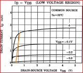
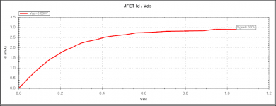
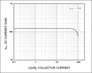
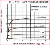
To function as a CCS it has to be baised in a horizontal part of the Id/Vd curves so that the Vd has no influence on Id.That's only the case for VDS>2V min.
Here every change in Vsd gives a change in Id,not much of a CCS.
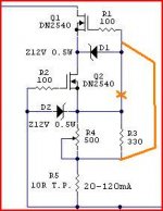
One could do it like this,to not deviate to much from the original.Even put the JFET back in,not only a resistor,since now there is 6V for it.
Mona
To function as a CCS it has to be baised in a horizontal part of the Id/Vd curves so that the Vd has no influence on Id.That's only the case for VDS>2V min.
Here every change in Vsd gives a change in Id,not much of a CCS.
One could do it like this,to not deviate to much from the original.Even put the JFET back in,not only a resistor,since now there is 6V for it.
Mona
Attachments
The bottleneck in Salas design lies in the very low voltage for the JFET.
To function as a CCS it has to be baised in a horizontal part of the Id/Vd curves so that the Vd has no influence on Id.That's only the case for VDS>2V min.
Here every change in Vsd gives a change in Id,not much of a CCS.
One could do it like this,to not deviate to much from the original.Even put the JFET back in,not only a resistor,since now there is 6V for it.
Mona
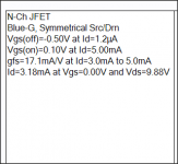
What you call a bottleneck is no bottleneck at all if the right jfet is used. Your solution has some significant drawbacks compared to simply choosing the right jfet that can give a very decent CCS while operating with approx 0.7V across it. So, one can choose the jfet with the smallest pinch-off (Vgs(off)) voltage (2sk170, 2sk117, j201) that can be found and done. It's not ideal, but it's better than other solutions; and obviously the people who made this choice have their definition of what "better" means.
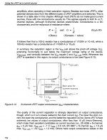
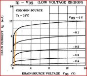
See page 154 in the attached images re Vds vs Vgs(off). The 2sk117 can have a Vgs(off) between 0.2V and 1.5V. So, if one can be found with Vgs(off) below 0.35V what is there to complain? Another trick is to put a LED in series with the bjt emitter to increase Vds. But build and see, in practice it hardly makes any difference, from what I've seen.
Attachments
In the Salas circuit the J-fet gets no more room then Vds+Vgs=0.6V.I don't no of any fet capable of operating in the flat portion of the Vds-Ids curves in those conditions.
Your sugestion of a LED where I put a zener can work to,best use a green one (or white),and then a J-fet again to get more loop-gain.
Mona
Your sugestion of a LED where I put a zener can work to,best use a green one (or white),and then a J-fet again to get more loop-gain.
Mona
You don't have to play it on the person,the question is,is it good enough for the circuit  .
.
Pick a workingpoint on the red line that gives a horizontal curve,if you can.
The less worst choice is the SK117
Mona
.Pick a workingpoint on the red line that gives a horizontal curve,if you can.
The less worst choice is the SK117
Mona
Attachments
2SA1381 (or KSA) shows ~0.6V VBE at 2 mA as biased in SSHV2. That is the ~VDS for the K117GR also.
That BJT has a flat HFE curve even at low Ic. If you got an E grade you will see HFE=150 on average.
For it to move +/-0.05V VBE will take max +/-mA Ic around its bias point. It won't swing there, but anyway.
And this is what that means to the example JFET's Id. You can get even lower Vgs(off) samples in GR by the way.
Attachments
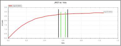
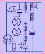
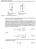
Dear Salas,I think you made an error during the developement of this project.Origionally,right connected,the 12V zener was nessesairy to protect the J-fet.
Now it sits parallel on the b-e diode of Q5 because the base is wrong connected.The result is that Vbe=Vds+Vgs.With the base at the source it's Vbe=Vds,much better.The workingpoint lies on the new red line depending on the current trough 2x68k = Vout.
Mona
Now it sits parallel on the b-e diode of Q5 because the base is wrong connected.The result is that Vbe=Vds+Vgs.With the base at the source it's Vbe=Vds,much better.The workingpoint lies on the new red line depending on the current trough 2x68k = Vout.
Mona
Attachments
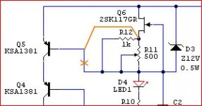
When the trimmer is at 0 we get the equivalent of the connection you draw, then Vgs=0 and the Jfet is biased at Idss.
When its not set at 0, the gate remains tied at the bottom of the trimmer's resistance.
A small feedback voltage is provided to the gate, the bias goes below Idss but even better regulated.
Its like having a different output conductance Jfet under Vbe then. The trimmer's end is the effective source pin connected to the BJT's base.
Its still a CCS. Plus trimmer controllable.
- Home
- Amplifiers
- Power Supplies
- Simplistic MosFET HV Shunt Regs