Look up the Thread that gives all the data you should need to draw up your short list for devices depending on their duty.
I seem to remember that VAS and Driver and Output each have their own list.
Most transistors have comments attached.
This work was done by one of our Members.
Can anyone point to his name or his thread? It is not in Articles.
I seem to remember that VAS and Driver and Output each have their own list.
Most transistors have comments attached.
This work was done by one of our Members.
Can anyone point to his name or his thread? It is not in Articles.
More progress
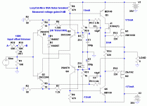
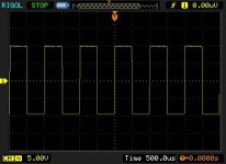
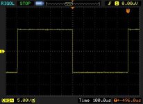
The input offset trimming tweak proved very helpful, now the prototype is tamer for offset drift. The bias in the drivers and output remains steady after the CCS tweak. Here is what schematic I run by now, including 1kHz 20VP-P square wave screens. -3dB gain frequency is 1MHz.
The input offset trimming tweak proved very helpful, now the prototype is tamer for offset drift.
The bias in the drivers and output remains steady after the CCS tweak. Here is what schematic I run by now, including 1kHz 20VP-P square wave screens. -3dB gain frequency is 1MHz.Attachments
The article "gain Structure" explains it all very adequately.
Why do you state something quite unjustifiably in an effort to put down another Member?
If we have a line level Signal of XmVpk and we require that maximum signal to never exceed YmVpk at the speaker terminals then the system gain is simply the ratio of one over the other.
It can rarely if ever be as you have stated.
Nice design, but awfully big gains.. I would only use gains like 10 to 15dB, max 20dB for power amp. I know it's not "traditional" solution, but still makes sense in 95% of the setups by making gain structure more reasonable.
I wanna use my buffers on it from a turntable. Do that with 10-15dB.
I wanna use my buffers on it from a turntable. Do that with 10-15dB.
Well that explains it then.
")
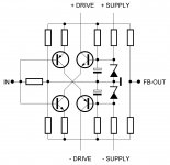
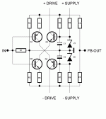
SSA basic front end
I couldn't get how the front end works (I very weak at understand audio amplifier, beginner learning phase)
So I would be appreciate if you could explain in the way which music input is flowing through components for each halfwave.
I couldn't get how the front end works (I very weak at understand audio amplifier, beginner learning phase)
So I would be appreciate if you could explain in the way which music input is flowing through components for each halfwave.
Attachments
Can I use bf471/472 instead of 2sc3788 on low impedance version? http://www.diyaudio.com/forums/solid-state/193923-simple-symetrical-amplifier-118.html#post2755474
SSA Explanation
This circuit elegantly permits use of bipolar semiconductors at the input with conjoined bases. Normally this creates problems in current feedback symmetrical circuits where feedback is injected into the emitters since by joining the input bases of opposite gender devices we shift the DC points of the emitters +/-0.6V, which is very awkward for feedback.
The emitters of each of the input devices Q1 and Q2 (see attached image with designations) are fed with a small current via R4 and R5. These resistors are connected to a DC voltage source of just under 2 volts through R6 (pos) and R7 (neg). The primary voltage source to power these positive and negative biasing networks is formed by R8/Z1/C1 (positive +15V supply) and R9/Z2/C2 (negative -15V supply).
Thus, with Q1/Q2 bases connected and bias via R1 to ground, we have a constant DC current supplied via R4 and R5 to Q1/Q2 respectively. The value of this current is determined by the values of R4, R6 (pos) and R5, R7 (neg) and stands at a few milliamperes.
Feedback is taken from the FB-OUT node via R10/R11 to the inverting input (the emitters of Q1 and Q2) via R4/R5. Notice the fb is split in two, one network for each half of the circuit. The voltage divide function for this fb voltage is supplied by R2/R3 and is identical for both halves.
Now, what happens to a signal input?
Let us stick with a positive going signal; negative is simply the reverse.
As the base of Q1 (and Q2) rise, it moves Q1 emitter closer to its voltage source, reducing current through R4. Q2's emitter, however, moves further from its voltage source, increasing current through R5. This is the important step for a positive input and is the important current here, since it passes through Q3, which is wired as a cascode with its base firmly held at +15V, so that Q3 offers no resistance to this current change at all, passing it to the upper gate/source resistor (470R) labelled +DRIVE on the schematic.
With more voltage dropped across the 470R gate/source drive resistor on the upper output device, it switches on harder, and passes more current to the load. The drain potential on this device settles to whatever voltage is required at the load to permit this output device current to flow, so the load is activated, and the speaker voice coil passes a positive current.
With the load now having a positive voltage on it, the opposite (inactive) output device is not involved here; its drive is reduced, so it may even turn off... offering no contribution to the load current, which is supplied only by the active output device. With a positive current flowing through the load, a voltage is created across it, and this is fed back to the input as feedback for the amplifier. Fb is passes back to the input devices, both Q1 and Q2, via their respective fb network resistors, R10-R4-R2 and R11-R5-R3.
The voltage appearing at the load will thus present back to the emitters of the input devices, modifying their transonductance (that is, how hard they turn on or off) by varying the voltage at the junction of R2-R4-R10 and R3-R5-R11. This reflects back to the emitters, so that the drive on the load is no more and no less than that required to multiply the output over the input by the gain ratio of (R10+R2)/R2 and (R11+R3)/R3, which are identical of course to ensure identical gain for each half cycle.
This circuit is a bipolar adaptation of one of Jean Hiraga's circuits from the late sixties, Le Monstre, IIRC. It is a clever solution because it structures the DC voltages at the feedback nodes to allow use of bipolar devices, since jfets of opposite gender are harder and harder to source. It appears to have a good distortion profile and is clearly an inspired design - hats off to Andrew!
Cheers,
Hugh
Attachments
Last edited:
This circuit is a bipolar adaptation of one of Jean Hiraga's circuits from the late sixties, Le Monstre, IIRC.
Thanks for the great explanation, Hugh.
Knowing that the front end is very sensitive to power supply, and that the Hiraga uses battery, do you think the attached schema is correct for implementing front end power supply?
Attachments
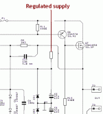
Yes, Jay, it looks fine, though details are not given HOW it's regulated.
Most of these simple circuits, including the FetZilla, are highly sensitive to rail supply, and care must be taken with in the SSA to ensure that the +/-15V supplies are very quiet, since they are directly connected to the feedback node.
Hugh
Most of these simple circuits, including the FetZilla, are highly sensitive to rail supply, and care must be taken with in the SSA to ensure that the +/-15V supplies are very quiet, since they are directly connected to the feedback node.
Hugh
Hugh, thanks alot. Thats the very explanation I'm finding !
Just curious, aren't R8 also responsible for bias voltage drop for positive half ? Since the supply voltage need to pass through R8, then R6, finally R4 ?
Just curious, aren't R8 also responsible for bias voltage drop for positive half ? Since the supply voltage need to pass through R8, then R6, finally R4 ?
The emitters of each of the input devices Q1 and Q2 (see attached image with designations) are fed with a small current via R4 and R5. These resistors are connected to a DC voltage source of just under 2 volts through R6 (pos) and R7 (neg). The primary voltage source to power these positive and negative biasing networks is formed by R8/Z1/C1 (positive +15V supply) and R9/Z2/C2 (negative -15V supply).
Yes, Jay, it looks fine, though details are not given HOW it's regulated.
Why is that important? I thought I can use any regulators that I used for opamp based linestage. At least, Salas' one I think can be the best.
Actually, I was prepared to have response about the redundant zener. But I think it will not do any harm to the sound. The R-C-Z will be there on the board, plus another MKP, while the regulator will be on another board.
Hi Guitar,
R8/R9 simply drop the rail voltage down to the +/-15V required by the fb network, nothing more. They don't actually influence the vb node voltage division; that is done by R10/R6/R2 and R11/R7/R3 respectively. The static +/-15V does not influence the gain equation; it cancels out completely and serves only to bring the fb node to a point higher and lower than the emitters of the input devices so that they can switch on and pass current.
Jay,
The type of regulation used is important, since its impedance characteristics do influence the sound quality. I like to use simple emitter followers to power circuits, since their Zout reduces with increasing current and they are very stable. Conventional regulators are feedback devices, and their output voltage is not always stable under dynamic conditions, since feedback ALWAYS requires compensation because it introduces phase shift.
I've been looking at the distortion profile of Elvee's amp. I'm not that happy about it, actually, H2 is only about 40dB below for +20dB output, not low enough.
Cheers,
Hugh
Member
Joined 2009
Paid Member
Thanks for the great explanation, Hugh.
Knowing that the front end is very sensitive to power supply, and that the Hiraga uses battery, do you think the attached schema is correct for implementing front end power supply?
Jay, the front end is in two parts, the input stage (which is also the feedback error amplifier) and the VAS. In your picture it looks as if you are proposing a regulated supply to feed the Zener diodes only. The zener diodes are a type of shunt regulator, acting to regulate the supply voltage to the cascode devices and provide a stable anchor point for the voltage at the fdbk node. Providing these diodes are bypassed by good quality and sufficiently large capacitors I don't see any merit in regulating the power supply to them. You want the zener diodes to have a very low impedance but as they have their own intrinsic impedance it's beneficial to lower their effective impedance by placing caps in parallel with them. Achieving a low impedance over the audio range means using low ESR caps and with a large value because their impedance increases at low frequencies. Lazycat recommends 1000uF; your 47uF (IF I'm reading it right) seems a tad small to me. The impedance of the cap can be calculated from resistance in Ohms = 1/ (2 x 3.141 x frequency in Hz x capacitance in Farads).
Regulating the power supply to the VAS is a different option and I'm not sure if you proposed that ? I think this is a worthwhile thing to do if you want the best performance because it not only reduces noise getting in from the PSU but provides better isolation between channels if they share a transformer. But there are a number of things you have to consider - Google is your friend for some initial reading. In the end I decided that for my version I would take the easier path of isolating the VAS power rails from the rest of the amplifier with diode-resistor-capacitor. If I were to regulate the VAS rails, I find the concept of a shunt regulator more attractive than a series regulator.
Last edited:
Hi Bigun, from reading Hugh explanation about how the front end works, I saw that both the supply and feedback goes to the same node, i.e. the emiter of Q1 and Q2, thus the supply must be quiet.
In original circuit, the regulator is the zener, R=1k and C=47uF. I just want something better than that. Of course, shunt type regulator is already written on stone for hard core DIYers.
The 47uF might be too small, I don't know. The circuit is from this thread, as proposed by Lazycat and Nico Ras. But I think Salas used 1000uF here. Me? I don't care with calculation. I know that the final sound is not only determined by the value of this capacitance. Each capacitor brand has different other parameters than capacitance. What I will do is try some of good caps I have on hand (Black Gate 1000uF/680uF/470uF/47uF, Sicorels, and many others), and pick the one that gives best sound. But as a standard procedure, I always parallel with Solen (Black) MKP, 100/220/330nF, if I can hear the difference. With certain good elco, lower value of MKP usually preferred.
Can you explain what you mean here? Of course my original question was to seek for the best possible regulation, whether it is front end, VAS, or even the driver, if it will affect the performance.
In original circuit, the regulator is the zener, R=1k and C=47uF. I just want something better than that. Of course, shunt type regulator is already written on stone for hard core DIYers.
The 47uF might be too small, I don't know. The circuit is from this thread, as proposed by Lazycat and Nico Ras. But I think Salas used 1000uF here. Me? I don't care with calculation. I know that the final sound is not only determined by the value of this capacitance. Each capacitor brand has different other parameters than capacitance. What I will do is try some of good caps I have on hand (Black Gate 1000uF/680uF/470uF/47uF, Sicorels, and many others), and pick the one that gives best sound. But as a standard procedure, I always parallel with Solen (Black) MKP, 100/220/330nF, if I can hear the difference. With certain good elco, lower value of MKP usually preferred.
Regulating the power supply to the VAS is a different option and I'm not sure if you proposed that ? I think this is a worthwhile thing to do if you want the best performance because it not only reduces noise getting in from the PSU but provides better isolation between channels if they share a transformer. But there are a number of things you have to consider - Google is your friend for some initial reading. In the end I decided that for my version I would take the easier path of isolating the VAS power rails from the rest of the amplifier with diode-resistor-capacitor.
Can you explain what you mean here? Of course my original question was to seek for the best possible regulation, whether it is front end, VAS, or even the driver, if it will affect the performance.
The 47uF might be too small, I don't know. The circuit is from this thread, as proposed by Lazycat and Nico Ras. But I think Salas used 1000uF here.
There is 330uF Nichicon in mine, and 1000uF PanaFC in the other one, the 27dB gain that my friend runs. Its just what I had handy for the proto, but I have some 470uF/16V Panasonic Pureism to test later, when I will copy to stereo and start listening in the main system speakers if the whole thing will prove safe on expendable old computer plastic speakers.
The '15V and 2V drop' is only an example value ? is it variable with different component or fixed ?........ The emitters of each of the input devices Q1 and Q2 (see attached image with designations) are fed with a small current via R4 and R5. These resistors are connected to a DC voltage source of just under 2 volts through R6 (pos) and R7 (neg). The primary voltage source to power these positive and negative biasing networks is formed by R8/Z1/C1 (positive +15V supply) and R9/Z2/C2 (negative -15V supply).
I'm not sure how this R8/Z1/C1 structure works, so should I look for (the name, so I can study on it)
Can't quite get it how does R1 plays the role in Biasing. Only knows that R4/R5 is limiting the current to base for biasing.Thus, with Q1/Q2 bases connected and bias via R1 to ground, we have a constant DC current supplied via R4 and R5 to Q1/Q2 respectively. The value of this current is determined by the values of R4, R6 (pos) and R5, R7 (neg) and stands at a few milliampere.
So to say, the the feedback Global type ? any local feedback ?Feedback is taken from the FB-OUT node via R10/R11 to the inverting input (the emitters of Q1 and Q2) via R4/R5. Notice the fb is split in two, one network for each half of the circuit. The voltage divide function for this fb voltage is supplied by R2/R3 and is identical for both halves.
To confirm I understand this, I typically repeating with my own word, see if i'm correct.As the base of Q1 (and Q2) rise, it moves Q1 emitter closer to its voltage source, reducing current through R4. Q2's emitter, however, moves further from its voltage source, increasing current through R5. This is the important step for a positive input and is the important current here, since it passes through Q3, which is wired as a cascode with its base firmly held at +15V, so that Q3 offers no resistance to this current change at all, passing it to the upper gate/source resistor (470R) labelled +DRIVE on the schematic.
During positive halfwave, the voltage at base Q1 increase (toward voltage source), thus lowering the Adc(for bias) that WAS across emitter, possibly turn off it. While opposite happen to Q2, the current increase.
For me the Q3 and Q4 looks like a permanently open door, permit the flow of Q1/Q2 to DRIVE anytime.
Curiosity came out : Since it has no resistant, Why not directly connect +/-DRIVE to collector of Q2/Q1. (eliminate Q3 and Q4)
Why called the 470R(drive) as gate/source drive resistor, why not put a speaker ?
Can't quite understand the red highlighted part, how/why will it "increase the current" ?With more voltage dropped across the 470R gate/source drive resistor on the upper output device, it switches on harder, and passes more current to the load. The drain potential on this device settles to whatever voltage is required at the load to permit this output device current to flow, so the load is activated, and the speaker voice coil passes a positive current.
So to say, the Q1 would turn off(depends on preset Iq) during the peak/increasing of positive signal, and Q1 will turn on during the decreasing(weak portion) of positive signal, then proceed to negative halfwave signal ? (opposite reaction) The nature of 'SSA front end' ?With the load now having a positive voltage on it, the opposite (inactive) output device is not involved here; its drive is reduced, so it may even turn off... offering no contribution to the load current, which is supplied only by the active output device. With a positive current flowing through the load, a voltage is created across it, and this is fed back to the input as feedback for the amplifier. Fb is passes back to the input devices, both Q1 and Q2, via their respective fb network resistors, R10-R4-R2 and R11-R5-R3.
Just for curious, won't the voltage at topnode of R6/R7 (DC voltage source below 2V) will go{leak} into FB-OUT ? (Perhaps is to modulate the voltage for changing transconductance ? but how.... would be glad if you could explain further details , like using magnifying glassesThe voltage appearing at the load will thus present back to the emitters of the input devices, modifying their transonductance (that is, how hard they turn on or off) by varying the voltage at the junction of R2-R4-R10 and R3-R5-R11. This reflects back to the emitters, so that the drive on the load is no more and no less than that required to multiply the output over the input by the gain ratio of (R10+R2)/R2 and (R11+R3)/R3, which are identical of course to ensure identical gain for each half cycle......
 )
)Does the gain controlled using R2/R3 ? (reduce Feedback) doesn't R4/R5 responsible for any gain controlling ? Won't supply voltage escape to ground through R2/R3 ?
Member
Joined 2009
Paid Member
Hi Bigun, from reading Hugh explanation about how the front end works, I saw that both the supply and feedback goes to the same node, i.e. the emiter of Q1 and Q2, thus the supply must be quiet.
I'm not arguing against regulation, each designer has to decide on his/her own preferences for the tradeoffs that exist. I saw very little additional value in regulating the supply to the zener diodes as the diodes are themselves a regulator - it's like regulating the supply to a regulator - diminishing returns. If you were to regulate the supply you may as well consider getting rid of the zener diodes since they add their own noise. The fdbk node voltage is set by the current flowing through the relevant resistors - and this current flow depends on the voltage from the zener's. It does benefit from being as quiet as possible and a zener is a fairly crude shunt regulator - but it is simple and this alone can be a real benefit. The noise generated by the zener can be shunted away by the bypass capacitor and here you really do want to use a good cap, low ESR and large value.
As the PSRR of the amp is sensitive to the size of these caps, using small value caps will mean that the PSRR is lower and a regulated supply will add more benefit. Being a symmetrical amp with dual rail supply it has good PSRR against symmetrical rectifier ripple - but if you have more than one channel running off the same supply any Class B waveforms on the supply rails will be asymmetrical and the PSRR is then much lower - you get channel to channel cross talk. Regulated supplies and/or large caps help here.
Can you explain what you mean here? Of course my original question was to seek for the best possible regulation, whether it is front end, VAS, or even the driver, if it will affect the performance.
The SSA design has the zener diodes supplied from the same power rail as the VAS. If you regulate the power rail to the VAS and leave the zener diodes in place drawing their current from it, then you regulate both the input stage and the VAS with one regulated supply. Regulating the rails to the VAS will help keep PSU noise out of the VAS stage.
Last edited:
- Status
- This old topic is closed. If you want to reopen this topic, contact a moderator using the "Report Post" button.
- Home
- Amplifiers
- Solid State
- Simple Symetrical Amplifier