For the moment, is i'm not wrong, there is 4 + variants from L.C.. One with FETSs inputs and BJT output, one with BJT input and FETSs output, one pure BJTs, and one called BIGBT with BJT inputs, and lateral Mosfets followed by power BJT output. Plus two working variants from contributors.So many options....which one to build?")
The variants are for inputs, symetrical or not. All are in the "simple" (is beautiful) concept. In progress, if i had understood well, is a state of the art version (not so simple) witch, i hope, will be followed by top of the art other versions ?
I'm happy that you had appreciate my idea of a symmetrical input. I hope i don't bother-you too much with ideas and adaptations (i killed my boss with patents when i was young). It appears that this nice SSA way to bring current feedback to the inputs is marvelous and can be applied everywhere, even on existing amplifiers like mine (with your help). A very attractive and simple way to demonstrate with very little mods on any existing amp the advantages of the negative feed back principle. I believe that near all the major inputs configurations had been explored, and each time, adaptation was simple and elegant. Congratulation again.Esperado I am glad to see that you are very interested in this un/balanced version cause it enables you customization to your needs.
Right now I am working on High Performance unbalanced version and I looks very promising, will report later.
At the same time I am thinking about the elegance of the later SSA balanced sch which is also very appealing to me to make it in near future.
Also all symmetrical differential input designs can be easily turned into full balanced version with global negative current feedback. A whole new space of an experimentation opened, me just love it.
I hope you will take in consideration my remarks about power supplies, and i hope you will have a look to my simple and efficient protection, as simple and obvious (once understood) than your SSA architecture. I Would like to share with you a complete protection/soft power on/off circuit, mine is working since 25years, and has proven so many times his accuracy.
I think it could be time to put somewhere on line the different working versions for easier reference to the readers witch could be updated continuously. I'm at your disposal to manage-it under your authority, if you like. Sad the forum does not allow to modify any time the posts, witch would allow that kind of things, updating the first post with last schematics.
And i'm very exited about your "hight performance" version to come. A fantastic works in a so fast progress...
About current in the driver stages for fets and mos fets, i'm sure you can read better than me the datasheets about the hole of gate capacitance in the high power fet devices. I lie on you ( mine are a little less 1nF), lazy to calculate the current at 10mHz. and there is always the solution to reduce the impedance/bandwitch with a gate resistance in case of oscillation during edges. ;-)
Last edited:
Hi igor0203
First define your expectations than try to read from the start ...
I am sure you'll find something useful here, otherwise just interesting reading.
Well I'm looking for something better than ICEpower 125ASX?
Member
Joined 2009
Paid Member
Stop-by sometime for sharing the info ... wish you successful built of your new amp.
I'm sorry for a fast developing thread, what can I do, ideas just pops out ... it will be a looong winter.
We'll know by December whether I am able to build it or not. And it's good to see a fast moving thread, lots of ideas and contributors, just how the forum should be.
I'll track my build here: http://www.diyaudio.com/forums/solid-state/196973-tgm5-all-bjt-simple-symmetric-amplifier.html
LC, I have simulated the PSRR. For 1V/50Hz ripple in both supplies the output ripple is +-7mV. Good/bad?
I think only a listenning test can tell.
What did you find? Did you test it with an unregulated supply?
A good measure in reality is 100Hz frequency output component in spectra present at idle condition. Usually there is cca. 200mV ripple riding on rails DC and the output should be at least 80 dB lower.
At my SSA amp I found it extremely quiet regarding all kinds of noise at output.
If you replace zener diodes with LM431 shunt regulator you would certainly get more -dB of PSRR. Also front-end could be supplied separately, gaining more isolation from the output stage rails ripple.
At the moment I see no reason to do any of that measures. Look Shaan, first try it and always recheck in reality what simulator's claiming. Attached schematic is my proposal for splitted power supply if you want to do it.
Attachments
Last edited:
A good measure in reality is 100Hz frequency output component in spectra present at idle condition. Usually there is cca. 200mV ripple riding on rails DC and the output should be at least 80 dB lower.
At my SSA amp I found it extremely quiet regarding all kinds of noise at output.
If you replace zener diodes with LM431 shunt regulator you would certainly get more -dB of PSRR. Also front-end could be supplied separately, gaining more isolation from the output stage rails ripple.
At the moment I see no reason to do any of that measures. Look Shaan, first try it and always recheck in reality what simulator's claiming. Attached schematic is my proposal for splitted power supply if you want to do it.
Thanks for all this info LC, you are kind as always.
Yes I always build what I sim. I simmed the opamp-type first, built it then. Reality matched the sim results(which I can measure, i.e. sound from the speaker and readings from the digital multimeter,
 ).
).I plan to run the input stage from the same unregulated supply(with the zeners of course) and if(IF) there is a "little" hum, I'll just quadrouple the reservoirs.
I have at hand all the components and now doing hFE matching of the BJTs. Expect good things.
P.S. I'm quite amazed by the bandwidth curve. ~10MHz. Chance of ending up with a power radio oscillator?
Last edited:
Prefer green LEDS at 5mA to Zener or TL431. 7 each will suffice. And it will glow.
As there is 6 15V zener and two green led on board, the zener replacement with green led will induce presence of 50 green led per board...sure that will glow
 and that only for mono mode, image in stereo configuration.....100 green led.....that will be a good green lamp for traffic jam regulation.....
Marc
Ok I have problem with biasing it does not mater how many times i turn trimmer nothing happens, can be the problem with IRF parts, the truth is I newer get to the end just to lets say 150R On Base collector resistance ?
Help I need somebody help. trimmer is now full turned proximately 260R between Base Collector of VBE transistor green led glowing DC OFFSET 25 mV without trimming, but I can not bias output transistors (MJL 3281A/1302A no changes turning pot 0mV redaing
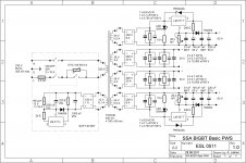
PCB is
Attachments
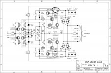
Help I need somebody help. trimmer is now full turned proximately 260R between Base Collector of VBE transistor green led glowing DC OFFSET 25 mV without trimming, but I can not bias output transistors (MJL 3281A/1302A no changes turning pot 0mV redaing
PCB is
Please measure as many voltage potentials you can and put their values in sch. Than I can help you out.
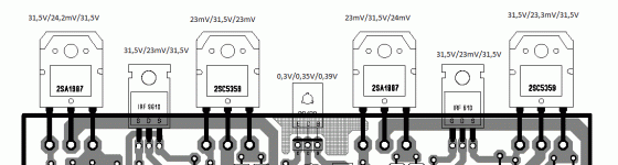
measure the Vbe multiplier voltage.
That voltage should change as you alter the Vr.
The voltage on Vbe multiplier does not change when turning trimmer correction they are 0,3V/0,35V/0,35V
The voltage on Vbe multiplier does not change when turning trimmer correction they are 0,3V/0,35V/0,35V
My simulations show that it may help to change the two 100ohm resistors to 120ohm (I did see the same problem).
Vbe multiplier base to emmiter voltage is 90mV, so it is not in function, like it wouldn't be there.
In this case you should have full Vgs voltage (maximum bias current!) on mosfets (across 1k gate resistor) but the reading is zero. So you probably don't have +/-15V on zeners or input/cascode transistors are mixed-up. Input cascode's collector current should be present so voltage reading across 1k gate resistor should be there. If the voltage on gate 1k resistors is zero that means you have some mistake in input stage cause input collector current is not present. Please recheck NPN/PNP positions, voltage across zeners, input pair colletor current (voltage across 10 ohm emmiter resistors should be app. 45mV, voltage across 1k gate resistor should be 4,5V), etc.
The correct start-up phase should be zero ohm between base to collector of the Vbe transistor and than slowly increasing resistance by turning trimmer to get app. Vce=1,2V (22mV across 0,22ohm output emmiter resistors).
Last edited:
My simulations show that it may help to change the two 100ohm resistors to 120ohm (I did see the same problem).
That won't help at all.
Vbe multiplier base to emmiter voltage is 90mV, so it is not in function, like it wouldn't be there.
In this case you should have full Vgs voltage (maximum bias current!) on mosfets (across 1k gate resistor) but the reading is zero. So you probably don't have +/-15V on zeners or input/cascode transistors are mixed-up. Input cascode's collector current should be present so voltage reading across 1k gate resistor should be there. If the voltage on gate 1k resistors is zero that means you have some mistake in input stage cause input collector current is not present. Please recheck NPN/PNP positions, voltage across zeners, input pair colletor current (voltage across 10 ohm emmiter resistors should be app. 45mV, voltage across 1k gate resistor should be 4,2V), etc.
The correct start-up phase should be zero ohm between base to collector of the Vbe transistor and than slowly increasing resistance by turning trimmer to get app. Vce=1,2V (22mV across 0,22ohm output emmiter resistors).
as far as a can see input transistors are ok bc550c/560c Q3 is BF471 Q4 BF472 voltages on zener diode will measure later
- Status
- This old topic is closed. If you want to reopen this topic, contact a moderator using the "Report Post" button.
- Home
- Amplifiers
- Solid State
- Simple Symetrical Amplifier