Hi Mike,
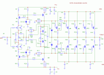
I am working on the exact same circuit (without the current sources) as you describe, except with mosfets and a cascoded input fets.
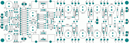
MikeW even made PCB's for me and I have a working prototype which still needs some work. I will try to post the schematic this evening.
I will have to disagree with most of you about the validity of this circuit, I think that it has a lot of potential and have to agree with Kuei Yang Chan on this one..........Sorry!
Regards,
Jam
I am working on the exact same circuit (without the current sources) as you describe, except with mosfets and a cascoded input fets.
MikeW even made PCB's for me and I have a working prototype which still needs some work. I will try to post the schematic this evening.
I will have to disagree with most of you about the validity of this circuit, I think that it has a lot of potential and have to agree with Kuei Yang Chan on this one..........Sorry!
Regards,
Jam
AKSA said:Mikeks,
I find myself agreeing with you. I have built and tested them all, and a standard diff pair, with single ended VAS using a CCS as collector load, is the best overall gain block I've ever tested.
True in all respects.....
I fear the main reason the generic (Thompson) design is derided by audiophiles is it doesn't look as 'sexy' as the so-called complimentary designs, or push-pull TIS configurations....
Goes to show...looks aint everything...!!!

Thanks all for the positive comments.
Hi CBS240,
I really designed this around the IR MOSFETs which, if driven in the Vas/SF fashion would waste about 7V of output c.f. < 2V here.
All the other transistors are small signal 500mW high Hfe such that the EF driver stage can be 300MHz and Hfe >500 needing only 20uA base drive current for 10mA Class A standing current and dissipates avg 35mW!
Hi Kuei Yang Wang,
I have covered complementary single ended FET (and BJT) input stage in the patent application as a possible configuration. But it is more problematical for DC offset even in an AC coupled feedback config and really requires a servo which adds complexity. I might add that the complementary FET se input stage you favour will result in much higher THD (due to poorer transconductance /gain) and degraded PSRR due to higher collector impedance of BJT.
The higher power version GB300D uses a 'modulated bias' standard cascode with BJTs and can be FETs.
However, due to the ready availability of monolithically matched FET cascode chips, I prefer to develop the nested/compound feedback design using one such chip for the front end to a bipolar discrete stage as above.
Hi Hugh,
I have explored all manner of variation in the resistors being bootstrapped and leave that subjective stuff to constructors.
Hi Lumanauw,
If you do a sim of the topology you'll find that the size of the bootstrap C's directly affects the LF PSRR but the topology does it for the mid and high.
My aim here was to derive the topology that could provide a viable alternative to the conventional - without the glaring weaknesses. I don't expect it to be acknowledged - even Douglas Self could not acknowledge that PSRR was a problem, even when using a regulated supply dropped THD from 0.04% to 0.006% from memory. If that's not the flag... But maybe, just maybe, Wireless World were right when they sub-titled my article on PSRR "Audio Distortion - Holy Grail Located!"
High Mikeks, If your conventional topology is to work as well you will need more cost/complexity and even in it's basic form is more wasteful of power - it's a dinosaur!
Cheers,
greg
PS thanks for all the emails guys.
Ok Greg,
I am convinced about high frequency operation of your circuit, it is really good, But having complementary pairs of mosfets at output poses on problem....If someone feels to use this circuit above 1KW++ level .....There would be a Hell with P-channel Mosfet, as they are not available in high power versions, thats why i am die-hard "Cieling Fan" of nvmos.......")
Could you please elaborate in a better view , how the power supply hash doesn't contaminates this circuit as in traditional circuits with seperate VAS?
K a n w a r
I am convinced about high frequency operation of your circuit, it is really good, But having complementary pairs of mosfets at output poses on problem....If someone feels to use this circuit above 1KW++ level .....There would be a Hell with P-channel Mosfet, as they are not available in high power versions, thats why i am die-hard "Cieling Fan" of nvmos.......
Could you please elaborate in a better view , how the power supply hash doesn't contaminates this circuit as in traditional circuits with seperate VAS?
K a n w a r
Hi amplifierguru ! I saw your schematic . VAS is a common collector stage . Iq through VAS will depend on +-Vcc , .Will this decrease PSRR ?
Are you using Multisim professional version ? I only has got student version . This version is too bad but orcas pspice can't measure PSRR
Are you using Multisim professional version ? I only has got student version . This version is too bad but orcas pspice can't measure PSRR
Hi Kanwar,
Yes it's really been designed to get the most from IRFP p and N channel but it might be possible to configure a CFP for the P channel.
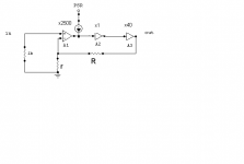
The earlier pics I showed the sim results for the 2 topologies and the gain breakdown for the diff'l - Vas- EF/SF conventional approach, showing the inherent PSR at the diff'l /Vas node due to the Rl/Zc divider.
Below pic shows the very different gain breakdown within the loop of the new topology. It can be seen, if we look back from the output at, say, 20V rms output, the bootstrapped load sources 0.5V signal so PSR is relative to this whereas with the very high gain of the Vas, for a similar output level, the signal level at the Diff'l out/Vas in node is 160 times lower giving a poorer ratio of PSR intrusion to signal level. One way of looking at it. In effect increasing A1 while reducing A2A3 is the key - putting less of the gain after the intrusion point and more of the gain before.
hope that helps.
Notice that the drivers turn on to pull the MOSFETs off ?
Cheers,
Greg
Yes it's really been designed to get the most from IRFP p and N channel but it might be possible to configure a CFP for the P channel.
The earlier pics I showed the sim results for the 2 topologies and the gain breakdown for the diff'l - Vas- EF/SF conventional approach, showing the inherent PSR at the diff'l /Vas node due to the Rl/Zc divider.
Below pic shows the very different gain breakdown within the loop of the new topology. It can be seen, if we look back from the output at, say, 20V rms output, the bootstrapped load sources 0.5V signal so PSR is relative to this whereas with the very high gain of the Vas, for a similar output level, the signal level at the Diff'l out/Vas in node is 160 times lower giving a poorer ratio of PSR intrusion to signal level. One way of looking at it. In effect increasing A1 while reducing A2A3 is the key - putting less of the gain after the intrusion point and more of the gain before.
hope that helps.
Notice that the drivers turn on to pull the MOSFETs off ?
Cheers,
Greg
Attachments
hi,guru
good idea!
before about 10 years,I saw that a janpanese DIY expert had a series articles of DIY amp which less sensitive for the power supply in MJ magazine.his method is same as yours by increasinng the gain of the input stage and decreaing the gain of VAS....But he more likes complemetary topology
IIRC,his last one of this type amp is complemetary J-FET (about +/- 70 Vcc) cap couple+ MOSFET source follower(about +/-30V Vcc),only one stage for amp volt ....his topology is so simple!
sorry for my direct words.....in my eye,
your amp=japanese DIY amp vari + EF + boostap+ Nelson Pass A5 without active current source
regards
X.G.
good idea!
before about 10 years,I saw that a janpanese DIY expert had a series articles of DIY amp which less sensitive for the power supply in MJ magazine.his method is same as yours by increasinng the gain of the input stage and decreaing the gain of VAS....But he more likes complemetary topology
IIRC,his last one of this type amp is complemetary J-FET (about +/- 70 Vcc) cap couple+ MOSFET source follower(about +/-30V Vcc),only one stage for amp volt
....his topology is so simple! sorry for my direct words.....in my eye,
your amp=japanese DIY amp vari + EF + boostap+ Nelson Pass A5 without active current source
regards
X.G.
Hi Thanh,
I said I liked things simple - yes it's easy to see the standing current in the Vas is sensitive to the supply, but, being such a late entry point (so much gain x2500 before) any effect is small. It simply maintains the right Vgs to ensure the MOSFETs are doing what the FB loop tells them. The current in this EF Class A stage at 8-10mA is typically 10 times whats needed by the MOSFET gate C.
If the supply goes low, optput needs is lower.
I've been using CircuitMaker which has a downloadable student version. You can do a bode plot with the sig gen on the input then move it to modulate one or other or both supplies, then the bode plot magnitude is the transmission of a signal on the supplies, to the output i.e. PSRR (but must add amp gain , say 30dB to the down figures as that's the gain for a signal at the input).
hope that helps,
Greg
Hi XG,
Thanks.
MJ magazine - I don't know that.
I tried KIS (keep it simple) AND achieve great efficiency, low distortion and DC coupled option all at less cost than conventional 'garden variety' design.
"your amp=japanese DIY amp vari + EF + boostap+ Nelson Pass A5 without active current source"
Haha - don't tell me I'll have NP on my back?
Cheers,
greg
amplifierguru said:If your conventional topology is to work as well you will need more cost/complexity.....
I really fail to see the truth in this....
amplifierguru said:........and even in it's basic form is more wasteful of power....
How so...

amplifierguru said:
..........degradation in PSRR (bode plot).........
due to the 3200 x miller C paralleling with the A1 load Z ...........
real improvement can be obtained by reducing the gain of the Vas e.g. with R to ground.
This intuitively raises the signal level at the injection point relative to the PSR injection.
This is probably why the low TIM followers perceive a benefit in loading the Vas.
I am sorry Greg, but low PSRR is dependent on having high feedback, and therefore foward-path gain particularly at ripple frequency.
This foward path gain is (to a first approximation) the product of transadmittance gain (input stage), and transimpedance gain (second stage, alias the lamentably misnamed 'VAS').
The later, (TI gain), is roughly the product of current gain, and the net load at the second stage-output buffer interface.
Therefore, loading down the output of the second stage (TIS), can NOT cause, or even appear to cause an improvement in PSRR...
amplifierguru said:
It becomes fairly obvious that we are just fiddling at the edges of a flawed topology and that the Vas is 50% of the problem.
D. Self has demonstrated clearly that this need not be the case....
Hi Mikeks,
You seem to have misinterpreted -
"..........degradation in PSRR (bode plot).........
due to the 3200 x miller C paralleling with the A1 load Z ..........."
This refers to the effective multiplication of the miller C by the gain of the Vas stage to appear across the diff'l load which makes for a lower impedance path at HF from power supply to the Vas input node, of the voltage divider with the output Rc (collector impedance) of the diff'l stage.
"real improvement can be obtained by reducing the gain of the Vas e.g. with R to ground. "
this refers to the practice of resistive loading to ground of the Vas collector to lower gain of the stage which reflects ,say, 320C (10 timers lower) back to the diff'l load. The signal level will then be 10 times higher at the Vas input, for the same output so PSRR is improved 20 dB! Could be perceptible!
Douglas Self doesn't seem to understand PSRR.
As far as cost/complexity goes - i took the same parts and needed a beefier Vas driver stage (more expensive), higher voltage supplies (more expensive power x'former and PS C's) for the same power and more intricate compensation (more C's,R's) to come close to 0.005% at 20KHz to match.
Power efficiency was poorer for the Vas type requiring larger heatsink due to extra MOSFET waste voltage, driver heatsinking and x'former size for more current/voltage. Then there's the overbuilding (wasteful) necessary to compensate for the POOR PSRR - double x'former VA and double PS C - all for 6dB audible improvement.
Check your intrusion equations using A1 A2 A3 with injection at A1A2 node and you will find , for a given OL /CL gain the PSRR is proportional to A1/A2A3.
Cheers,
Greg
Hi, Amplifierguru,
Could it be the "current drive mode" that makes the good sound? Someone once wrote that it is different between an amp that gives straight voltage amplification output (Vout=kxVin) and an amp that gives current output, where (Vout=ZxIout), this is because speaker is Z not R, so current drive mode is different than ordinary voltage drive.
Is the topology works good in class AB?
http://www.diyaudio.com/forums/attachment.php?s=&postid=732896&stamp=1127896282
http://www.diyaudio.com/forums/showthread.php?postid=734107#post734107
I believe lumanauw was alluding that the output stage (and thus the whole amp) is a transconductance stage (U in; I out), contrary to a source follower output stage, before closing the feedback loop.amplifierguru said:I don't think so. I've measured and sim'd output Z and it's very low.......
As the transconductance is high, after closing the feedback loop, of course you get low output Z.
But eg. Mauro Penasa stated that this topology sounds better because of better interaction with real loudspeaker loads. There was also a thread in which this was discussed.
Tino
jam said:
Comments anyone?.....................This is still a work in progress.
One question: what is the circuit close to Vgs complemetany multilier to geter with feedback? I mean R49/50/51/52 and C13. A combination of lacal feedback from VAS and from output stage?
regards
- Status
- Not open for further replies.
- Home
- Amplifiers
- Solid State
- Simple Killer Amp!