Hi Hugh,
I missed you there.
Hi CBS240,
Sure you can go to all this complexity - but I'm emphasising the simple solution, topologically(?).
It's not about Fizzzz in the background. It's the distortions from the PS that are generated and enter during dynamic operation, that add the edge.
DC is not an issue. The design can be AC coupled for similar tolerances, but my preference is for DC coupling , so I'm not listening to capacitor smearing and that involves setting at 0mV cold, running it up to see where it goes when hot. If it's +30mV then you reset it at cold for -15mV so it averages around 0mV. That's the setting up on DC coupled. Not much pain, for no FB cap.
But just as you're not listening to the PS with all you're PS mods, I'm not listening to it with more simplicity than a conventional simple Vas but I canget some 50W more power or headroom for less cost and 1/10th the THD at 10KHz.
Cheers,
greg
Hi Anthony,
No worries. The conceptual topology is posted http://members.dodo.com.au/~gregball/guru_003.htm
There are some 7 claims in the patent application covering the bias adjustment, DC offset adjust and thermal compensation. The devils in the detail. Obviously there are zeners on the gates to supply. All the details on the functional schematics are in the kit.
Note the 30mW 200MHz+ small signal drivers that pull the gates
off.
Luckily I have an audiophile lawyer mate who's really litigious and into international IP. A pit-bull.
Cheers,
greg
amplifierguru said:Sure you can go to all this complexity - but I'm emphasising the simple solution, topologically(?).
If you want to emphasize the simple solution topologically, as I said over in jam's split portion of the thread, it don't get much simpler than this:
An externally hosted image should be here but it was not working when we last tested it.
So I might well say, "Sure, you can go to all this complexity - but..."
")
se
Congrats Greg..on your mos##amp , I like it...
On More thing you too use Circuitmaker for simulation ..is'nt its great....
By the way if i want to parallell more mosfets at output,shouln't they require an extra buffer to compensate high drive loss at high frequencies...
K a n w a r
On More thing you too use Circuitmaker for simulation ..is'nt its great....
By the way if i want to parallell more mosfets at output,shouln't they require an extra buffer to compensate high drive loss at high frequencies...
K a n w a r
amplifierguru said:Hi Anthony,
No worries. The conceptual topology is posted http://members.dodo.com.au/~gregball/guru_003.htm
There are some 7 claims in the patent application covering the bias adjustment, DC offset adjust and thermal compensation. The devils in the detail. Obviously there are zeners on the gates to supply. All the details on the functional schematics are in the kit.
Note the 30mW 200MHz+ small signal drivers that pull the gates
off.
Luckily I have an audiophile lawyer mate who's really litigious and into international IP. A pit-bull.
Cheers,
greg
Hi Gregory,
so, when are you going to file an associated application to gain any intellectual property rights for the invention?

btw, It's a neat design, I like it!
Cheers Michael
Hi Steve,
You're a #U*&^% genius! Why didn't I think of that.
Hi Kanwar,
Thanks, sometimes it's the simple things. You should see the bias/offset/thermal solutions!!! Yeah, I think I like circuitmaker - except when it breaks tracks when you make changes. Very frustrating trying to fault find a straight line that reads different at both ends.
Gate current draw is about 1.5mA/pair at 10KHz full power from an 8-10mA biassed driver giving a fair slew margin. But at 30mW on a small signal pkg, what the hell - I could run them harder!
So it's R2R and GREAT PSRR - I can use a 170W x'former and 15,000uF a side for a 150W monoblock - and it'll hit 210W before clip (rms) on music crest factor. And it's 100 times less sensitive than a Vas type to those supplies so they can bounce around.
Cheers,
greg
amplifierguru said:in an energy efficient world of the future (should've been yesterday!)...
... we'd all be using digital amplifiers....
dave
Greg,
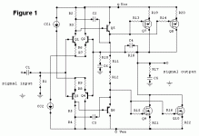
HEXFET's, do you use (IRF) vertical FET's in the output? In such cae I wonder wethere you have Q5 and Q6 thermaly tied to the output FET's Q7, 8 9 & 10 because of their positive tempco, if thermaly tied together it will compensate a bit for thermal runaway in those output FET's.
When thinking of thermal compensation, it hits me that also if Q2 and Q4 would be thermaly connected to the output transistors mentioned above will give thermal compensation as well.
And there's more posibilities too actually when one get's passionated thinking over it...
The above applies to the attached schematic here below fetched from your link in your earlier post in this thread, hope that's ok for you Greg.
What is the overal gain for the whole circuit before FB is applied?
Tell me about C2 and C3, are they small values in order of pF's or so, or is it such a high value it can be considered as a bootstrap capacitor?
Cheers Michael
Attachments
Hi Michael,
I designed it around IRFs! The 3-4V gate voltage. In fact the tests I did covered 100 prs of 2 batches and determined tempco which are compensated for in the final. Yes - looking for the tempco comps was fun and, if you look at the blurb on my website I indicated a variety of tempco comps. At least three.
Q5,6 only provide a fraction of the measured tempco so I have devised simple, largely existing, alternatives.
The C's 2 andf 3 are serious bootstrapps. They are larger than needed for response boost , for PSRR boost!
Done the hard yards.
Cheers,
Greg
Hi Greg,
I really like your topology. I believe it solves many of the usual problems...... And the use of emitter followers to drive the gates is very appealing to me, and the simple use of a bootstrap enables constant current operation, high linearity, while accommodating very good offset control.
Try using different values for the complementary bootstrap caps. It will sound quite different and you might even like it.......
Yes, it looks very good, congratulations!
Just how vigilant is your lawyer, and how does he perform in out of state jurisdictions???
Cheers,
Hugh
Guys,
Schematics in post #6 is absolutely OK. It is amplifier with NEGATIVE feedback. Darkfenriz and MikeB are mistaken. Common base stage in cascode DOES NOT INVERT the phase of the signal. If it is so hard to see it just draw schematics of usual cascode and try to prove 360 degrees phase inversion.
Schematics in post #6 is absolutely OK. It is amplifier with NEGATIVE feedback. Darkfenriz and MikeB are mistaken. Common base stage in cascode DOES NOT INVERT the phase of the signal. If it is so hard to see it just draw schematics of usual cascode and try to prove 360 degrees phase inversion.
Konnichiwa,
I rather like it in many ways.
But I retain that the differential Amp's are troublesome.
If you can do me the honours and just forget for a moment that they are "differential amplifiers", which in your case is not the case.
Let me restate for you your Input/VAS topology:
"A pair of rail symmetrical single ended amplifiers are used as voltage amplifiers with the feedback signal applied to the emitters using emitter followers."
One may ask why not return the feedback signal to the emitter without buffering? And why use BJT Inputs?
If do that we arrive at any one of a number of variation of Mosquite/Buzzquito/Zenquito et al which are popular with the French, with rail symmetric differential or rail symmetric single ended frontends....
http://perso.wanadoo.fr/jm.plantefeve/
Sayonara
amplifierguru said:No worries. The conceptual topology is posted http://members.dodo.com.au/~gregball/guru_003.htm
I rather like it in many ways.
But I retain that the differential Amp's are troublesome.
If you can do me the honours and just forget for a moment that they are "differential amplifiers", which in your case is not the case.
Let me restate for you your Input/VAS topology:
"A pair of rail symmetrical single ended amplifiers are used as voltage amplifiers with the feedback signal applied to the emitters using emitter followers."
One may ask why not return the feedback signal to the emitter without buffering? And why use BJT Inputs?
If do that we arrive at any one of a number of variation of Mosquite/Buzzquito/Zenquito et al which are popular with the French, with rail symmetric differential or rail symmetric single ended frontends....
http://perso.wanadoo.fr/jm.plantefeve/
Sayonara
Konnichiwa,
It will work if we do it that way....
There is BTW a very neat possible qiescent current compensation scheme possible in this circuit (not drawn), by making the current sources suitably active with a DC loop back from the source resistors, bootstrapping could also be employed, but is probably not needed.
Sayonara
Allexx said:Sorry, I was wrong because for feedback signal injected into source it will be positive...
It will work if we do it that way....
An externally hosted image should be here but it was not working when we last tested it.
There is BTW a very neat possible qiescent current compensation scheme possible in this circuit (not drawn), by making the current sources suitably active with a DC loop back from the source resistors, bootstrapping could also be employed, but is probably not needed.
Sayonara
Hi Guru,
This topology was obviously designed for Fet outputs, I am using BJT's, mostly because I have plenty of them. I have grown fond of the EF stage instead of feedback pair(although yours is not exactly FP) for lower impeadence and thermal stability because of the very positive tempco of BJT's. But your topology idea could be used there as well i suppose. Drivers could probably be smaller. and freq responce will be higher. With FET's you loose the Vgs with SF, which is much greater than Vbe in EF, so it makes lots of sense to your design.
This topology was obviously designed for Fet outputs, I am using BJT's, mostly because I have plenty of them. I have grown fond of the EF stage instead of feedback pair(although yours is not exactly FP) for lower impeadence and thermal stability because of the very positive tempco of BJT's. But your topology idea could be used there as well i suppose. Drivers could probably be smaller.
and freq responce will be higher. With FET's you loose the Vgs with SF, which is much greater than Vbe in EF, so it makes lots of sense to your design. Kuei Yang Wang said:Konnichiwa,
It will work if we do it that way....
I don't think so. This time the feedback is okay, but your biasing is in
no way defined ! You can't have work 2 currents against each other
and expect a defined voltage... It would work if you replace the 2 ccs
with simple resistors or use your mentioned "dc-servo".
Sorry to be annoying,
Mike
Konnichiwa,
First, the circuit as drawn is meant as "simplified principle" diagram (as are all the others), secondly, if I select the CCS J-Fet's for sufficiently identical and appropriate Idss (the frontend FET's BTW also would need selection) I CAN expect defined biasing just fine. The exact biasing would then be determined by the frontend source resistors.
You are not annoying, you are merely completely wrong, which is no problem to me.
Sayonara
MikeB said:I don't think so. This time the feedback is okay, but your biasing is in no way defined ! You can't have work 2 currents against each other and expect a defined voltage...
First, the circuit as drawn is meant as "simplified principle" diagram (as are all the others), secondly, if I select the CCS J-Fet's for sufficiently identical and appropriate Idss (the frontend FET's BTW also would need selection) I CAN expect defined biasing just fine. The exact biasing would then be determined by the frontend source resistors.
MikeB said:Sorry to be annoying,
You are not annoying, you are merely completely wrong, which is no problem to me.
Sayonara
- Status
- Not open for further replies.
- Home
- Amplifiers
- Solid State
- Simple Killer Amp!