apexaudio, in another thread you have reported the existence of another BUZamp implementation, with a picture.
http://www.diyaudio.com/forums/solid-state/163159-150w-mosfet-amplifier-irfp250x2.html
I have taken the liberty to attach your picture here, in my post. Please see no offence. Can you provide us more info about this very interesting implementation :
- what is the thermal management ?
- how the two NMOS get put in parallel ?
- no source resistors anymore ?
- any over-current protection ?
Cheers,
Steph
Attachments
apexaudio, at the moment we are talking about 5 different implementations :
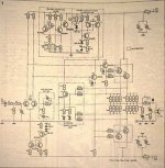
1 - the Siliconix VMOS, with current mirrors (F. de Dieuleveult) (see schematic above)
2 - the Siemens BUZ20 (Etienne Lemery) (see schematic above)
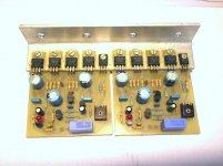
3 - the one that got reported by apexaudio (see picture showing 4 x BUZ21) (no schematic)
4 - the Elektor BUZamp (see picture showing 4 x BUZ23) (no schematic)
5 - the Apex N10 (apexaudio) (see schematic above showing 2 x IRFP250)
Will somebody provide the schematic of 3 and 4 before we end up in a mess ?
1 - the Siliconix VMOS, with current mirrors (F. de Dieuleveult) (see schematic above)
2 - the Siemens BUZ20 (Etienne Lemery) (see schematic above)
3 - the one that got reported by apexaudio (see picture showing 4 x BUZ21) (no schematic)
4 - the Elektor BUZamp (see picture showing 4 x BUZ23) (no schematic)
5 - the Apex N10 (apexaudio) (see schematic above showing 2 x IRFP250)
Will somebody provide the schematic of 3 and 4 before we end up in a mess ?
Last edited:
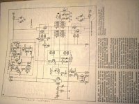
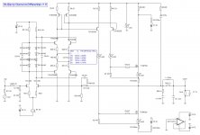
from apexaudio, here is the Elektor BUZamp, more or less readable. As expected, this is a bloated version of Etienne Lemery - Siemens BUZ20 amp, here with four NMOS. One can see the two thermistors in the 2nd differential pair current source. One must be for Iq regulation, and the other must be for thermal shut-down. One can also see an over-current protection, measuring the voltage drop on the low-value output resistors.
Attachments
Last edited:
Yes, (only three different) but by the use of the same PCB board. There are places for TO-220 outline (BUZ20) and TO3 (BUZ23) on the PCB:In Elektor was four different aplication with BUZ21 and BUZ23, try to find original.
1) 2x60W/4 ohms (+/-33V, 2xBUZ20)
2) 2x80W/4 ohms (+/-36V, 2x BUZ23)
3) 2x120W/4ohms (+/-40V, 4xBUZ20)
about
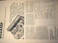
Power Endstufe mit MOSFET-Transistoren
you will find a high resolution schematic. From there you can also order copies from the original elektor article in German, published in the "Elektor plus 7" page 36-41.
But please note, there are two gleanings/advices to erratas from this project (at least in the German article):
1) 1/1988 page 41 (faulty marking of polarity by C10 in the schematic)
2) 4/1989, page 42 (confused outline from T12 and T13 on the PCB printing layout - confused base emitter marking)
I have heard, that this article also exist in the Dutch language (magazine "ELEKTUUR") If you want to have this paper in this language, check out the regarded elektuur special edition about
http://www.elektor.nl/ or
Elektuur DVD 1990 - 1999
or ask there:
Elektuur 1989 November Nr 313 Maandblad voor Elektronica. - Te koop op Tweedehands.nl
here some additional URLs concerning this BUZAMP:
Mathias hi-fi, Hifislutsteg (MOSFET)
www.elektronik.si :: Poglej temo - Izdelava oja?evalnika
Ampli MOS 200W
BUZ23 datasheet and Application Note, Data Sheet, Circuit, PDF, Pinout | Datasheet Archive
http://www.audiofanatic.it/Schemi/Tipo/Stato_solido/finali/pic_finaliSS/240W_MOS_BUZ23.jpg
Attachments
Last edited:
hello tiefbassuebertr,
many thanks for clarifying the BUZamp history within Elektor. The info you are providing, especially the corrections that got published afterwards by Elektor, is unvaluable. I guess this is another reason why the BUZamp concept never became a success.
Now that the schematics have been inventoried and clarified, let us now talk about the BUZamp concept. It is nearly time ...
In fact, the BUZamp is a kind of luck. Or mistake, maybe. Or waste, maybe.
Well, think about the way each MOS is getting the approx. 2.7V DC positive polarization, for operating near the threshold. The 2nd differential pair is biased with a DC current, entering the two emitters. Each collector thus pushes a DC current, half of the total current, into each NMOS gate resistor. If the NMOS gate resistor equals 1K ohm, one must thus operate each transistor in the 2nd differential pair at 2,7 mA roughly. The current source must be calibrated for precisely deliver 2.7 mA * 2 = 5.4 mA for getting the NMOS nearly conducting. So, now you understand how each NMOS gets a DC voltage bias manually adjusted using a trimpot, in order to reach his threshold. It looks fine ... on paper.
In the real world, thermal management must be exercised for avoiding a thermal runaway : the NMOS gets hot, the rest of the amp gets hot, and by misluck, the current source may also deliver more current. That's a vicious circle, kind of positive feedback, so if initially the current source was drifting by +5%, the NMOS may experience +250% more current at the end of the day. The effect reinforces the cause ! A thermistor must be used in a thermal negative feedback loop. When the NMOS gets hot, the resistance variation of the thermistor must induce a 6% decrease of the DC current that gets delivered to the 2nd differential pair, and then we get nicely stabilized.
But wait a minute.
What is the maximum drive obtainable, then, at the gate, when there is an audio signal on top of the approx 2.7 V biasing DV voltage ? THERE is THE issue of conventional BUZamps. Due to the fact that the 2nd differential pair is biased by a current source, the maximum obtainable current is equal to the current source current. No more ! And this value, because of the differential principle, never exceeds TWICE the collector current that gets pushed at rest.
You see the issue ? The amp has an inherent current limitation. The swing on the NMOS gates cannot exceed a voltage that's the double of the threshold voltage ! The swing will be 0V (2nd differential collector shut-off) ... to 5.4V (2nd differential collector in saturation).
So, if the averaged transconductance of the NMOS equals to 3 Siemens (from threshold to decent current like 8 amp), the maximum current that will be delivered by the MOSFET is equal to 2.7V * 3 Siemens = 8 Amp roughly.
If the load is 4 Ohm, this is only 32 V. Discount some voltage losses in the driver, and you quickly come to the conclusion that a BUZamp (fitted with a single NMOS pair) will never be able to swing a 4 Ohm more than + and - 30V (60 Vpp), even if you have a high voltage power supply like + and - 45V.
It looks crazy, but it is true. If you want to see more inherent current limitation, put a 2 ohm load. Then you will see the open loop gain of the BUZmos amp trying to raise the NMOS gate voltages, but due to the saturation of the 2nd differential pair, you will measure a dumb 5.4 V max swing, no more, on the NMOS gates. And the same 8 amp on 2 ohm load is a ridiculous + and - 16V swing (only 32V pp). Irrespective of the open loop gain. And irrespective of the power supply rails that may be + and - 42V !
This is the reason why Elektor made the BUZamp with four NMOS. The global transconductance gets doubled, and thus the max obtainable current gets also doubled.
This being said, everybody should be able to understand that the concept on the BUZamp is ill. The BUZamp is a waste of resource. You put two strong NMOS, but you can't swing the gates more than twice the threshold voltage ! That's ridiculous, especially when one realizes that swings like 10 V are really needed to get the NMOS fully conducting, with a low Rds (drain-source resistance). All NMOS factories are batteling for a low Rds. Nowadays, a Rds lower than 0.1 Ohm is easily obtained, with modern silicon. But you need a 10V swing at the gate.
So, dear friends, I'm sorry to tell you : you better stay away from BUZamp, especialy if you need to drive complex loads (capacitive stuff), or anything that's lower than a plain 8 Ohm purely resistive load.
End of my love story with BUZamp ?
Maybe not ...
How to get the 2nd stage being able to push far more than twice it's nominal operating current, in a linear fashion ?
I agree re the voltage swing on the gates of the output devices !
However if the 1 kresistors on the gates were replaced with constant current loads you could get a higher votage swing !!!
I am sure I have seen this done in the past it may have been in an RCA application note
regards Trev
However if the 1 kresistors on the gates were replaced with constant current loads you could get a higher votage swing !!!
I am sure I have seen this done in the past it may have been in an RCA application note
regards Trev
I have to be blunt here. These circuits look pretty unimpressive and just plain idiosyncratic in the extreme. This is classic late 70's early 80's stuff when designers were still struggling to make sense of what was needed to make a good amp - both in terms of topology and stability. As for Elektor and Mnr. Giesberts . . . . it was always a case of piling on the feedback and passing any concerns about stability off to the poor constructor.
Build these designs if you want to do something wacky, otherwise, in my view, the absolute breakthrough design from this era was the Leach amp, which ushered in the era of modern amplifier design - a beauty devoid of TIM, thermal runaway, with the focus on stability and ease of construction that has stood the test of time.
Build these designs if you want to do something wacky, otherwise, in my view, the absolute breakthrough design from this era was the Leach amp, which ushered in the era of modern amplifier design - a beauty devoid of TIM, thermal runaway, with the focus on stability and ease of construction that has stood the test of time.
let me now introduce a BUZamp variant, free form the inherent current limitation discussed in the previous post.
The trick is to rely on a sort of "current-feedback" topology, enabling the correction current to be an order of magnitude greater than the nominal operating current.
Some won't understand why this scheme can be called "current-feedback". I won't argue here. They will argue that the output voltage gets sampled and returned to the input, also in a voltage form, so why bothering people with "current feedback" stuff ?
Other people may say that the internals of the amp are not anymore Class A, becoming Class AB. This is true, also.
What really matters is to understand that massive current can now be pushed from the collectors of the 2nd stage (that now becomes the 3rd stage). The last stage is operating at about 8mA rest current, but in case of need, the collectors will push currents in excess of 30 mA. When this current meets the 470 ohm, a voltage of more than 12 V can appear, putting the MOS in total conduction, with a resisdual Rds that is no more than 0,1 ohm.
Voilà ! Magnifique !
I order to to this, we need to add 6 low current transistors on the native BUZamp implementation. Those 6 extra-transistors are arranged in a compact and symmetric way. Some educated people will recognize the Sansui Diamond-Differential arrangement.
Special attention must be paid to the resistor joining the two halves of the diamond. The value of this resistor defines the quiescent current of both NMOS at the output.
A value of 91 ohm gives 60mA Iq.
A value of 79 ohm gives 350mA Iq.
The amp that gets described here, has now a moderate open-loop gain.
Therefore, the 1Khz distorsion figure depends on the Iq that's chosen.
A low Iq of 60mA gives a THD of 0,147% 8 ohm load, 40Vpp 1 KHz
A high Iq of 350mA gives a THD of 0,029% 8 ohm load, 40Vpp 1 KHz
That's decent but not fantastic.
There is a boostrap scheme allowing the output to swing within 3V of the supply rails.
The 10 Khz square wave is very nicely reproduced with a slew-rate defined by the input low-pass filter (3,3K and 100p).
Actually, if one puts very sharp edges at the input, without a low-pass filter, the circuit is so rapid at turn-on, that it throws 15V spikes on the NMOS gates, that take a while to discharge along the 470 ohm gate resistor. This causes very brief but very high NMOS crossover currents in the order of 20 Amp, quickly destroying any normal power supply and any normal decoupling capacitor.
This very fast circuit NEEDS a low-pass at the input, in order to protect himself, and to protect the power supply and decoupling capacitors, from very harsh crossing spikes.
I repeat : those crossing spikes do occur because the 470 ohm on the gate cannot actively discharge the gate-source capacitance. One of the NMOS thus stays conducting for a while (say, half a microisecond), while the other NMOS already enters very rapid conduction. That's quite bad ... but is not likely to happen if a low-pass is put at the input.
Something to be tried is to add an active gate discharge circuit. The most simple one consists on a diode + NPN transistor.
The attached .zip file contains the Tina 7 T.I. schematic ready for simulation.
Comments and questions welcome,
Cheers,
Steph
Attachments
Completely agree ! Could it be the Siliconix implementation (schematic on post #1 above) is what you are referring to ?However if the 1 k resistors on the gates were replaced with constant current loads you could get a higher votage swing. I am sure I have seen this done in the past it may have been in an RCA application note
regards Trev
Agree ! Today, armed with simulations and experience, one realizes what kind of wreckage people could buy or DIY yesterday. A joke : could it be the QSC arrangement (6 kilowatt amp) is a kind of BUZamp fixed by a rocket scientist ?These circuits look pretty unimpressive and just plain idiosyncratic in the extreme. This is classic late 70's early 80's stuff
Do you think the - yet to be remembered - current source approach can improve the drive amplitude (more output power), and also speed-up the discharge of the gate capacitance (less crossover spikes) ?No not quite ! It did not seem so complicated as post 1 and only used 1 pair of output devices
No, it is not finished,
on March 19th 2010, kenpeter came with an interesting Soft Non-Switching version of the BuzAmp. See here http://www.diyaudio.com/forums/solid-state/163364-visch-not-visch.html in posts #7, then reviewed by elvee in post #10. Are you sure you understand the inherent limitations of the BuzAmp without curent sources in the MOSFET gates ? Are you aware that the voltage swing on the MOSFET gates cannot exceed twice the threshold voltage ? Do you realize this doesn't enable using the full potential of the output MOSFETs ? Quite a waste of ressources.
Me too, I stay stand-by, waiting for suggestions around a Siliconix-like modern schematic, using current sources in the MOSFETs gate drive. But forget about simplicity, in such improved schematic.
Cheers,
Steph
Last edited:
Less waste than class A.No, it is not finished,
on March 19th 2010, kenpeter came with an interesting Soft Non-Switching version of the BuzAmp. See here http://www.diyaudio.com/forums/solid-state/163364-visch-not-visch.html in posts #7, then reviewed by elvee in post #10. Are you sure you understand the inherent limitations of the BuzAmp without curent sources in the MOSFET gates ? Are you aware that the voltage swing on the MOSFET gates cannot exceed twice the threshold voltage ? Do you realize this doesn't enable using the full potential of the output MOSFETs ? Quite a waste of ressources.
Me too, I stay stand-by, waiting for suggestions around a Siliconix-like modern schematic, using current sources in the MOSFETs gate drive. But forget about simplicity, in such improved schematic.
Cheers,
Steph
Regards
-Are you sure you understand the inherent limitations of the BuzAmp without curent sources in the MOSFET gates ?
-Are you aware that the voltage swing on the MOSFET gates cannot exceed twice the threshold voltage ?
-Do you realize this doesn't enable using the full potential of the output MOSFETs ?
Yes, I studied that topic carrefully. I agree the first schematic whereas simple had some limitations.
I was wondering if some work was on going to tune it to the best. "You gave me your mud and I have turned it to gold" as said one french writter.

Yes Yes Yes !!! I'm still desesperatly seeking genuine, first hand info about how Siliconix was anticipating their VMOS line to be used in audio amplifiers.Are folks still looking for Siliconix DA76-1 "The VMOS Power FET Audio Amplifier"? I have it in a Siliconix catalog from March 1979.
- Status
- This old topic is closed. If you want to reopen this topic, contact a moderator using the "Report Post" button.
- Home
- Amplifiers
- Solid State
- Siliconix & Siemens NMOS amplifiers