Looking good, but the sandwiched drawing is throwing me off. Tubelab tried 5:1 for the crazy drive ratio, but he drove the tubes much harder to get gobs of power. Anyway, the output impedance is pretty high, so some local and/or global feedback will be needed.
Tubelab tried 5:1 for the crazy drive ratio, but he drove the tubes much harder to get gobs of power. Anyway, the output impedance is pretty high, so some local and/or global feedback will be needed.
Last edited:
Does anyone have a spice model for 6AV5 or better yet 6BQ6? The model i have doesn't seem to work. Also, will it be reliable to model this mixed G2+G1 drive?
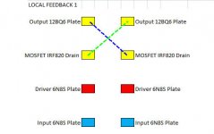
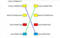
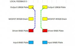
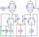
I have attached several scheme for local negative feedback. I hope i don't mess up the phase.. The feedback will be plate-to-plate like we can find on Alex Kitic's RH84 or Baby Huey. The dashed lines indicate the feedback resistor. Notice that some feedback will be cross-connected as each stage flips the phase. Do the schemes make sense? Help please. I prefer a mix between the shortest local feedback to drain (Option 1) and the long one (Option 2). Hope it's easy to understand.
I won't have to ask this if i have the Spice Model for the output tube and just play with some values in LTSpice. This is beyond my ability to imagine without simulation.
Attachments
Ayumi's library has one for the 6BQ6.Does anyone have a spice model for 6AV5 or better yet 6BQ6? The model i have doesn't seem to work. Also, will it be reliable to model this mixed G2+G1 drive?
Shown here for your convenience:
Code:
*
* Generic pentode model: 6BQ6_AN
* Copyright 2003--2008 by Ayumi Nakabayashi, All rights reserved.
* Version 3.10, Generated on Fri Jan 22 08:11:50 2016
*               Plate
*               | Screen Grid
*               | |  Control Grid
*               | |  |  Cathode
*               | |  |  |
.SUBCKT 6BQ6_AN A G2 G1 K
BGG   GG   0 V=V(G1,K)+-0.12830687
BM1   M1   0 V=(0.15009144*(URAMP(V(G2,K))+1e-10))**-1.2848724
BM2   M2   0 V=(0.53862432*(URAMP(V(GG)+URAMP(V(G2,K))/3.0739639)))**2.7848724
BP    P    0 V=0.0022372419*(URAMP(V(GG)+URAMP(V(G2,K))/5.7070648))**1.5
BIK   IK   0 V=U(V(GG))*V(P)+(1-U(V(GG)))*0.0018337045*V(M1)*V(M2)
BIG   IG   0 V=0.0011186209*URAMP(V(G1,K))**1.5*(URAMP(V(G1,K))/(URAMP(V(A,K))+URAMP(V(G1,K)))*1.2+0.4)
BIK2  IK2  0 V=V(IK,IG)*(1-0.4*(EXP(-URAMP(V(A,K))/URAMP(V(G2,K))*15)-EXP(-15)))
BIG2T IG2T 0 V=V(IK2)*(0.971797202*(1-URAMP(V(A,K))/(URAMP(V(A,K))+10))**1.5+0.028202798)
BIK3  IK3  0 V=V(IK2)*(URAMP(V(A,K))+1560)/(URAMP(V(G2,K))+1560)
BIK4  IK4  0 V=V(IK3)-URAMP(V(IK3)-(0.0017316916*(URAMP(V(A,K))+URAMP(URAMP(V(G2,K))-URAMP(V(A,K))))**1.5))
BIP   IP   0 V=URAMP(V(IK4,IG2T)-URAMP(V(IK4,IG2T)-(0.0017316916*URAMP(V(A,K))**1.5)))
BIAK  A    K I=V(IP)+1e-10*V(A,K)
BIG2  G2   K I=URAMP(V(IK4,IP))
BIGK  G1   K I=V(IG)
* CAPS
CGA   G1  A  0.6p
CGK   G1  K  9p
C12   G1  G2 6p
CAK   A   K  7p
.ENDSPlease don't mention AK's "P2P" in vain...The dashed lines indicate the feedback resistor. Notice that some feedback will be cross-connected as each stage flips the phase. Do the schemes make sense? Help please. I prefer a mix between the shortest local feedback to drain (Option 1) and the long one (Option 2). Hope it's easy to understand.
") Option 1 won't work, since the drains are tied to the B+ directly. Option 2 seem pretty far for a "local" FB, so option 3 looks the most promising. Have fun simming...
Option 1 won't work, since the drains are tied to the B+ directly. Option 2 seem pretty far for a "local" FB, so option 3 looks the most promising. Have fun simming...Sorry, I'm not trying to argue with you but it seems to me that for same power output, both Vg2k and Ig2 need to be lowered with the increase of Vg1k. Perhaps this is the point that I did not make clear enough.... but now it's scaled bigger as Vg2k also grows along with the increase of Vg1k. ...
Looking good otherwise, so, have fun and enjoy.

Last edited:
Just finished my #27 line stage and ready for the next step. It's either continue with the abandoned 6C33C OTL or try a screen drive amp since i just got my 12BQ6GTs, 12V heater version of 6BQ6GT. This thread is to lay out the design process with the hope that someone will catch any mistake before i go to far. I have finished several tube-related projects such as 6FD7 Class AB amp, 6LR8 SE amp, Aikido line stage and Futterman OTL headphone amp so while i am still a beginner in the world of tubes, i know enough how not to kill myself.
Been there; done that. You don't need screen drive to get that 40 -- 50W. You could easily nudge up V2K as the max screen voltage is specced at 200VDC. I didn't need to do this in the original design since the DC rail was a bit higher, and ~40W more than enough, so I stayed with the most common 150V of screen voltage.
Now, what is the target plate dissipation, Pdiss? 6BQ6GT is rated for max 11W Pdiss. I read that this is rather conservative and we can actually run it a bit hotter but i would like to stay within specs. I'll choose the usual 70% of max Pdiss which is 70% x 11W = 7.7W. Assuming Vak = 300V, this means Ia of 7.7/300 = 25mA. The actual Vak will be lower since i'm using mixed bias and end up with even lower Pdiss. This will be clear on the next paragraph.
Don't! For audio amplification, you can ignore that PD spec since that was for horizontal deflection duty (or if you were doing an FM xmtr project) which is a good deal more demanding than audio amplification. You can bust that spec without any adverse consequences. The bias point I used for Le Renard gives 17.5W with no trace of color on the plates, and I'm still using the same finals I installed in 2007. Hotter bias definitely improves both the loadlines and the sonic performance.
Help please. I prefer a mix between the shortest local feedback to drain (Option 1) and the long one (Option 2). Hope it's easy to understand.
It took awhile to find.. but here is a link to what Tubelab did for his "crazy drive".
I was thinking the same, perhaps ballpencil just wanted to try a screen/crazy drive design with whatever parts he had on hand. But using local feedback with 6N8P/6SN7 is going to be a problem - there's just not much lNFB, whereas the pentode driver such as the one used by Tubelab would work much better.You don't need screen drive to get that 40 -- 50W.
Miles' comment made me look for different datasheet and yes indeed one showed max Vg2k of 200V. The one i have from Sylvania has it at 175V.. but i guess keeping the screen drive has its merit: with the suboptimal OPT i have, it would be better to aim for more steeper loadline to cope with the lack of inductance. Aiming for the knee at Vg2k=200V needs something around Zaa 3k..while the one i chose is lesser at Zaa 1.7k.
An idea: I have a few of these module DC DC Boost Converter 8 32V 12V to ±45V 390V High Voltage ZVS Capacitor Charging | eBay
Though it would be useless as OPS plate supply, it would be great for G1-G2 driver supply. I already have the +12v heater supply to power it. It allows to drive G1 with another source follower and get something like dual drive Class AB2. I can then aim for even steeper loadline.
Ayumi's library has one for the 6BQ6
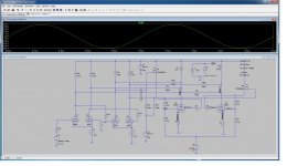
Shame on me for not searching there first. Thank you for this! It's very close to my calculations. Really have to give it to those Ayumi models. I can confirm at least by simulation that i'm getting my target. I chose Local Feedback method #3 and a local plate-to-grid feedback on the input LTP. With these, i'm getting 25Vp at the speakers with 1.8Vpp input. So.. that's about 40W. My output stage loadline prediction slightly differs on the max Ia. I predicted around 475mA while simulation gets 440mA.. not bad. I can see slight crossover distortion but overall things look great. It's a bit better after i increased bias current to 50mA for 14W of Pdiss.
Sorry for the spaghetti schematic but for convenience i highlighted the feedback part.
Attachments
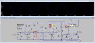
Here is the simulation for a very similar design I made last year. The sims all looked good so I built it. I could never tame the oscillation that it had, which claimed the lives of at least 10 mosfets. The prototype got robbed for parts before I ever really figured it out. It was admittedly a rather crude layout done when I had no lab and worked on the concrete floor in a cold garage.
Attachments
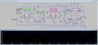
Thanks George! Your output to driver feedback resistor values is something that i really need to iron out this crossover distortion but unfortunately i can't afford more feedback there as i'm starting to move the clipping limit to the driver stage LTP and not at the output stage per usual. This low B+ is quite troublesome.
I did introduce another feedback loop from the driver to input LTP. It helps but i bet not as much as more feedback from the output would. With these values as shown, i'm getting 5.4% THD at 40W.
Something surprising came out when i tried to change the 30K+220K OPS to driver stage feedback resistor to 33K+180K for more feedback. THD actually increased to 5.9%. Not sure what happened..
Attachments
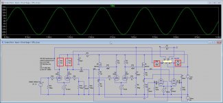
Thank you Anatoliy. If you're referring to global feedback from speaker output to input LTP, i would like to avoid it. That many ac-coupled stages can't be good for stability, would you agree?
I did try output stage plate to input LTP feedback if that's what you mean.. so like Scheme #2 on this post http://www.diyaudio.com/forums/tube...q6gt-amp-feasibility-study-3.html#post4614287 It definitely looks better! 3% THD at 40W.
I did try output stage plate to input LTP feedback if that's what you mean.. so like Scheme #2 on this post http://www.diyaudio.com/forums/tube...q6gt-amp-feasibility-study-3.html#post4614287 It definitely looks better! 3% THD at 40W.
Attachments
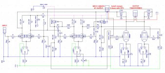
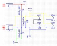
Rough layout attached. Inputs are welcomed.
HT2+ is for the driver & input LTP supply and on J5 there will be a jumper from HT+ to HT2+ if we are using the same supply as the output stage.
Tubes will be on the same side as the other components.. so most probably no tubes will stick out from the chassis. The only part that will need some heatsink would be the MOSFETs and they will simply be bolted to the chassis.
I've read that perfect current balance on toroid OPT does not necessarily mean no core saturation.. sometimes slight imbalance is needed. Is this true? In that case i will need to replace one of the LM317 current resistor with another trimpot. More hassle
Attachments
sometimes slight imbalance is needed. Is this true?
If both half - primary windings were identical (DCR, inductance, leakage inductance, and distributed capacitance) AND the tubes were perfectly matched for idle current, and Gm over the entire range of voltage and current they will see, then a perfect DC balance SHOULD coincide with minimum distortion over all audio frequencies and power levels.
In the real world, none of these things happen, much less all of them. The tubes will also age at different rates, making a good match now, a less than good match a year or two down the road. There are mismatches in most of these parameters, so that some DC imbalance often results in a better compromise than perfect DC balance. An AC balance control is also seen in some higher end amps (especially older ones).
I have noticed that most amps benefit from some DC imbalance, but toroidal OPT's are more sensitive to a static flux in the core. Even my $$$ Plitron's seem to like a few mA offset. I have included the ability to offset the bias in every fixed bias P-P amp I have made for this reason. It is possible to do this with a cathode biased amp, but I have not tried it. Some amps have included AC balance as well.
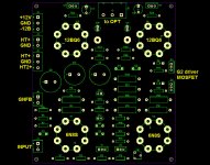
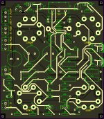
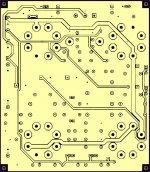
Finished routing the PCB. I followed George's suggestion to allow some bias current adjustment on one of the output tube and added 10R 1% resistors on each plate to measure current. I also added this 10R resistor highlighted on red square. I don't know what it's called but it helps to reduce THD considerably. I'm getting less than 2% THD at 40W. I think it helps to balance the output tubes and introduce a small degeneration. CMIIW.
As can be seen, i'm using ground plane and route all the power-related traces on the same side while signal traces on the other. I set 0.5mm clearance from the ground plane to other traces. I seem to recall that ground plane is not advisable in tube project PCBs? Is this correct?
Next target will be to getting all the parts, measure their physical dimensions and adjust the PCB as necessary.
Attachments
- Status
- This old topic is closed. If you want to reopen this topic, contact a moderator using the "Report Post" button.
- Home
- Amplifiers
- Tubes / Valves
- Screen Drive 6BQ6GT Amp - Feasibility Study