Have you pruchased the parts yet? If you have them in front of you while you are doing the layout you can measure and play with them. This helps things go faster, reduces mistakes. How about ground plane? I would use a coper fill on top and make the bottom solid copper with the two sides connected.
hi, maybe I missed something, but how do you intend to mount outputs onto heatsink ?
Hi,
I intend to mount them on right-angled aluminium brackets.
Regards
Your layout is not bad at all, components are to widely spaced, squeeze the whole amp, it will aid in shortening signal paths lengths. Your board can easily be shrunk by 50% and could look and work quite smartly.
U-Shaped heat sinks will not be good enough for your application, need something a little more substantial. Try changing R13/14 orientation because their far ends will short against the heat sink if it were mounted vertically. Also provide some securing mechanism for the heat sink, you cannot hang them off the transistors, you need some form of support.
U-Shaped heat sinks will not be good enough for your application, need something a little more substantial. Try changing R13/14 orientation because their far ends will short against the heat sink if it were mounted vertically. Also provide some securing mechanism for the heat sink, you cannot hang them off the transistors, you need some form of support.
P03A Image
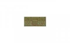
Here is an image of the P03A PCB from Rod's web site. The image is open to the public so I am not infringing Rod's copyright or IP. Normally, I would, and do, suggest buying Rod's boards, as I do, but a poor 15 year old needs a little bit of help.
You can use this image to use a guide for parts placement then link up the pins.
Attachments
You can be sure paranoid has been reading Rod's ESP site, and several times over! Elliott Sound Products - The Audio Pages (Main Index)
Ian, the reason I posted the image was because I thought if the OP had seen the PCB, he/she would have made an effort to copy, to a reasonable degree, placement of parts and work from there. Seems sensible to me; why re-invent the wheel?
Frank
PS Coffs Harbour is a lovely part of the world.
Frank
PS Coffs Harbour is a lovely part of the world.
Hi Francec
I support your suggestion, though it could be more easily viewed. I know too, that younger folk like to follow popular ideas like typical square format DX, NAP140 and other budget kits for small amps. This way, both amps might also share the heatsink and still fit in a smaller case. Perhaps though, this is not the right design on which to make such changes
Few schematics lead the eye to a wide format layout like the P3a until you get to multiple output devices. At least, similar things happen with local kid's designs here when they try to use free CAD software on simple amplifier circuits. I can only confirm that unless we do know more about design, it remains very important to follow Rod's layout, bearing in mind his challenge that it's going to be hard to beat his PCB for performance.
PS
Yep Frank, this area is like a magnet to your fellow Victorians. Many moved here for their midlife "C" change.
lol, they haven't worked out yet that it doesn't pay to be a sheep. Or as Brian said, in the best movie ever made, "you are all individuals" and the response "yes, we are all individuals".I know too, that younger folk like to follow popular ideas like typical square format DX, NAP140 and other budget kits for small amps.
For learning and understanding how to position components on a pcb, go to the Symasym designed on this forum. Look at its schematic and the pcb and understand what is going where and analyse with whatever your wisdom permits. Now u will find your pcb is resembling like that of the experts. Just give it a try.
At your age, u should be quite smart posting here.
Also remember, u have to lay the filter electrolytic capacitors as close as to the output transistors.
Gajanan Phadte
At your age, u should be quite smart posting here.
Also remember, u have to lay the filter electrolytic capacitors as close as to the output transistors.
Gajanan Phadte
I've read Rod's description and it is indeed possible to get away with not mounting the Vbe multiplier on the heatsink. In this case anyway.
Hmmm....
I also included a bias servo, using a pot and transistor. This was not mounted on the heatsink, since this would cause an instant negative thermal coefficient - as the amp gets hotter, Iq will fall, potentially so far that crossover distortion will occur. This is not a good thing, and I do not recommend it. The bias servo I used was done for convenience - I had a 20k trimpot to hand (well, a bag full actually), and the transistor is a standard BC549. I know its not elegant, and the values are not worked out properly, and ..., and, ... etc, but it works.
.....
Bias current also changes with temperature, so as the amp heats up, Iq will increase. This is not serious, and will only ever cause grief if the heatsink is too small. Such grief will ensue anyway in this case, regardless of whether the bias current is stable or not.
High Quality 60 Watt Power Amplifier
Hmmm....
For learning and understanding how to position components on a pcb, go to the Symasym designed on this forum.
Are you referring to this thread?
http://www.diyaudio.com/forums/solid-state/198500-symef-amplifier.html
Here is an image of the P03A PCB from Rod's web site. The image is open to the public so I am not infringing Rod's copyright or IP. Normally, I would, and do, suggest buying Rod's boards, as I do, but a poor 15 year old needs a little bit of help.
You can use this image to use a guide for parts placement then link up the pins.
I have already given a try to copy the layout earlier, but the pic distorts really very badly.....so its difficult to analyze!
Hi Francec
I support your suggestion, though it could be more easily viewed. I know too, that younger folk like to follow popular ideas like typical square format DX, NAP140 and other budget kits for small amps. This way, both amps might also share the heatsink and still fit in a smaller case. Perhaps though, this is not the right design on which to make such changes
Few schematics lead the eye to a wide format layout like the P3a until you get to multiple output devices. At least, similar things happen with local kid's designs here when they try to use free CAD software on simple amplifier circuits. I can only confirm that unless we do know more about design, it remains very important to follow Rod's layout, bearing in mind his challenge that it's going to be hard to beat his PCB for performance.
PS
Yep Frank, this area is like a magnet to your fellow Victorians. Many moved here for their midlife "C" change.
Absolutely....
For learning and understanding how to position components on a pcb, go to the Symasym designed on this forum. Look at its schematic and the pcb and understand what is going where and analyse with whatever your wisdom permits. Now u will find your pcb is resembling like that of the experts. Just give it a try.
At your age, u should be quite smart posting here.
Also remember, u have to lay the filter electrolytic capacitors as close as to the output transistors.
Gajanan Phadte
I have no idea what you are talking about, I tired searching 'symasym' but i didn't find anything pertaining to this topic...Please Elaborate!!
Are you referring to this thread?
http://www.diyaudio.com/forums/solid-state/198500-symef-amplifier.html
No, i'll starting reading it now.....
Thanks and Regards
I've read Rod's description and it is indeed possible to get away with not mounting the Vbe multiplier on the heatsink. In this case anyway.
As far as I know this is always the case with CFP/Sziklai output stage amps.
According to Self, only the drivers' temperature influence the quiescent current, and the multiplier should be on the same (small) heat sink as the drivers.
This cannot be the same heat sink as the output devices.
I have a p3a clone in service for about a year.
The drivers do not have a heat sink, but the multiplier is located just next to one of the drivers on the board, almost touching.
If I recall correctly, quiescent current is relatively stable after 15 minutes or so.
For sure there is no thermal run-away.
Here's a list of the symasym threads opened during 2011.
Oldest first
http://www.diyaudio.com/forums/soli...ks-pcb-builders-thread.html?highlight=symasym
http://www.diyaudio.com/forums/group-buys/156885-symasym-sequel-aaks-pcb-gb.html?highlight=symasym
http://www.diyaudio.com/forums/grou...buy-symasym-aak-modell.html?highlight=symasym
http://www.diyaudio.com/forums/soli...xt-generation-supersym.html?highlight=symasym
http://www.diyaudio.com/forums/solid-state/186617-help-symasym.html?highlight=symasym
http://www.diyaudio.com/forums/soli...uce-gain-symasym-5_3-a.html?highlight=symasym
http://www.diyaudio.com/forums/soli...hi-fi-amplifier-p12w4r.html?highlight=symasym
http://www.diyaudio.com/forums/soli...rf-noise-ehm-need-help.html?highlight=symasym
http://www.diyaudio.com/forums/grou...m-pcb-design-rev_1-3-a.html?highlight=symasym
http://www.diyaudio.com/forums/soli...-4-pcb-builders-thread.html?highlight=symasym
No symef among them.
As far as I know this is always the case with CFP/Sziklai output stage amps.
I'm not sure about that. The Vbe multiplier does not need to be on the same heatsink as the output drivers, but it still needs to track the temperature of the pre-drivers. Randy Slone explains this rather better than Douglas Self - I have just checked. Not mounting it on any heatsink can work, but not every time.
There are other considerations with Rod's circuit.
Here is the circuit (apologies if I transgress a forum rule about other people's circuits).
An externally hosted image should be here but it was not working when we last tested it.
Rod describes it as follows:
Those diodes in parallel with the bias servo (a.k.a. Vbe multiplier a.k.a. amplified diode) changes the picture a bit.The circuit for the bias servo (actually the whole amp, with some of the other mods I have mentioned elsewhere) is shown in Figure 1a - notice that I left the diodes in circuit as a fail-safe, since the servo I used will go open circuit if the pot wiper becomes disconnected (I strongly suggest that you do the same). In practice this works extremely well, and I can set bias current to anything I like.
But wait, there is more:
If there was a current source instead of the two 2k2 resistors the Vbe multiplier, things changes again. With the current through the bias servo constant, something has got to give.Variations in supply voltage will have an effect on Iq as well. I hadn't actually considered this much (I have never had one of these amps self destruct, and normally don't even bother measuring the quiescent current). The variation is caused because the Class-A driver current is not derived from a true current source, but is a simple bootstrapped circuit. Since the current must change with voltage, so must the voltage across the diodes (or bias servo).
The mathematics says that the relationship between transistor current, voltage and temperature is

where
- IE is the emitter current
- VT is the thermal voltage kT / q (approximately 26 mV at 300 K ≈ room temperature)
- IES is the reverse saturation current of the base–emitter diode (10−15 to 10−12 ampere)
- VBE is the base–emitter voltage
Last edited:
Here's a list of the symasym threads opened during 2011.
....
No symef among them.
Thanks for the answer.
Just typing 'symasym' into the forum search brought up a list of seemingly unrelated threads. The SYMEF one is the only one that comes even close. It does go through a PCB design exercise. That's why I asked the question.
I should have used the advanced search.
- Home
- Amplifiers
- Solid State
- Rod Elliot P3A Layout - Critics