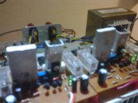
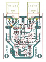
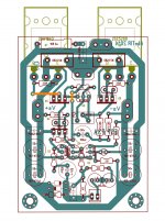
Good Day Sir Ian sir how about this""" is this ok' sir?...No heatsink for the driver transistors or thermal coupling for the bias transistor? That will be "interesting" under power, or is that just a part finished amplifier?
Hint: bias will be irregular and too slow in response, without enough thermal coupling to the driver(s).
Being right next to the output emitter resistors, they will have more affect on bias than the drivers. This is not a good layout for a CFP amplifier design. It may be possible to move the large resistors under the board and simply kink an aluminium strip heatsink to fit to the correct side of the righthand driver transistor (as in pic 3, above). This should solve the problem of what looks like reverse facing drivers.
Thermal coupling can be done by having a small bias transistor in close proximity, as you see on Rod Elliott's original PCB or a larger one fixed to the same heatsink as in AlexMMs layout. If you use TO126 transistors for all 3, as you have, it would be much better to couple them all to the same small heatsink, which could be a simple strip of 3mm aluminium, perhaps 15 mm wide.
Attachments
Hi desertstorm
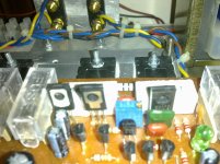
I see you now have the drivers bolted to separate chunks of aluminium heatsink. That may be OK for dissipating heat but the requirement is to couple the 3 devices with 1 heatsink. It may also be OK to couple to only 1 driver or place a TO92 size Q9 very close to the driver. Either way, it must be at the same temperature as the drivers.
Check the last paragraph in my post again, as you quoted.
I can't be certain what your PCB arrangement is, but I assume the bias transistor, Q9 is just in front of the bias pot, VR1. This means it is not close to the drivers, Q5,6. It seems to be obscured by the pot. so it can't sense the driver temperature.
It wont be easy to fix this PCB because the thermal coupling wasn't taken into account in the layout. See post #441 pics here
To do do this properly you need to use a single strip of aluminium, long enough for all 3 devices to bolt onto - or just clamp Q9 with a small strip of metal. If the PCB won't allow this, I think you'll have to start again, as did John Bali.
Member
Joined 2009
Paid Member
Yes, just buy a cable that has a headphone plug on one end for the ipod and on the other end a connector for the P3a (such as an RCA plug). I bought one from my local consumer electronics shop for a few dollars and I use an ipod to test out my amplifiers from time to time. The handy part is that you don't need a volume control or pre-amp as they are all included inside the ipod.
D
Deleted member 148505
Thank you Rod for posting your designs! Others too! Interesting reading!
Could one (I know it would be time consuming and not practical unless diy) follow a schematic for this or any of the SS amp designs posted and do it P2P in a way to have it work just as well if done with the best PCB designs? Maybe it would have to be done sort of 3D instead of on one plane to work the best. Perhaps on a CU sheet as a ground plane or a heavy CU ground wire threaded around.
Just thought it might be possible as it works well with tubes & Rod's doesn't have many parts so might be a good start.
Last edited:
I could say P2P for any discrete power amplifier is a "bad idea" but I guess you're hoping to save a buck whilst learning this the hard way. Whatever the construction method , wiring has to follow general layout rules and guidelines specific to class AB amplifiers. With 10 or fewer components in a Chip-amp, this is not so difficult, given the limited physical options. With 20 discrete components and no layout or roadmap though, serious problems with hum, noise, distortion and instability can break loose.
Layout faults might be fixable to a degree but often, they are never resolved because it is difficult to understand, pin down and remedy them without special instruments and training. PCBs of proven good performance capability are actually the key to realizing the amplifier's potential more simply. That's why you should start with such a good, defined layout - a reference.
Layout faults might be fixable to a degree but often, they are never resolved because it is difficult to understand, pin down and remedy them without special instruments and training. PCBs of proven good performance capability are actually the key to realizing the amplifier's potential more simply. That's why you should start with such a good, defined layout - a reference.
From time to time i find my self repeating the same things I hope people learn from it .
Αddicted costumer with the sound of P3A already owns one of them nicely made dual mono huge sinks and caps come into my shop asking me to design a PCB that will include one ch of P3A and one power supply but designed to work length wise in order to fit them behind speakers .
The size available was very little something like 4cm wide but the length could be usable up to 60 cm ...
Done my best regarding the pcb try to follow most of audio rules regarding distribution of signal grounding and so on and on given the available size But truly the amplifier never played as good as the original board .
keep in mind that obviously schematic and pcb had no errors , also the BOM was complete and made with quality parts +goodies like 100uf extras bypassing and so on .
So amplifiers are pcb depending , pcb can and will make a change in overall performance probably marginal but still existing
Personally i would never risk to get the pcb designed to be dual layer like the one above since this one is never tested ( full and real tests with proper instruments and by no chance anyone's opinion that will say " I 've been listening to it and sounds really fine) as a complete device especially now that features things i don't like such is a ground plane ...
Been making so many PCB's for the P3A to find out and learn the reasons that pcb will work better in this amplifier so obviously i will be very skeptic since my targets for this amplifiers are the highest ...
Kind regards
Sakis
hi all, sorry for disturbing, but someone tried to install the power transistors; drivers transistors and transistor quiescent current (BD 139 version) on the same heatsink? and leaving the transistor Q4 on a heat sink out from the rest? oscillation would bring complications and / or thermal stability to the team?
hi all, sorry for disturbing, but someone tried to install the power transistors; drivers transistors and transistor quiescent current (BD 139 version) on the same heatsink? and leaving the transistor Q4 on a heat sink out from the rest? oscillation would bring complications and / or thermal stability to the team?
Your post doesn't make much sense for starts which lay out you are talking about
Member
Joined 2009
Paid Member
...Perhaps on a CU sheet as a ground plane or a heavy CU ground wire threaded around.
I have used a double sided board for my version (http://www.diyaudio.com/forums/solid-state/245619-tgm8-amplifier-based-rod-elliot-p3a.html) and this approach allows me to keep good grounding discipline, low inductance paths for decoupling capacitors, keep high impedance nodes away from interference and to keep current loops small. It sounds superb.
Like Sakis thinks, it is not clear without posting your schematic/layout. I'll guess that you want to change the heatsinks around to suit your layout.hi all, sorry for disturbing, but someone tried to install the power transistors; drivers transistors and transistor quiescent current (BD 139 version) on the same heatsink? and leaving the transistor Q4 on a heat sink out from the rest? oscillation would bring complications and / or thermal stability to the team?
Let's make some guidelines:
1. The design is not the usual emitter follower (EF) type. It's a CFP design where bias thermal control is taken from the drivers, not Output Tx
2. Q9 needs to be close to, or even mounted with the drivers on their own heatsink, so that bias is maintained correctly.
3. The output stage is separate and should be separate from the drivers so as not to wrongly affect the bias control.
4. Q4 only needs a heatsink if you are going to risk the amplifier safety with 43V rails. The smallest T0220 size heatsink or similar will suffice.
Read some of the posts in this thread where it is shown several times
Also read the ESP project and notes at Rod's website: 60-80W Power Amplifier
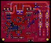
I guess my posted P3A pcb design here http://www.diyaudio.com/forums/solid-state/164756-p3a-comparsion-table-long-47.html should have been posted in this thread. ") I have come up with a new lay-out variation, and following Ian's and Bigun suggestion. It has a new look, both input stage of this design were totally re-arranged.
I have come up with a new lay-out variation, and following Ian's and Bigun suggestion. It has a new look, both input stage of this design were totally re-arranged.
0ne thing for sure my P3A is going to be a slow build
I have come up with a new lay-out variation, and following Ian's and Bigun suggestion. It has a new look, both input stage of this design were totally re-arranged. 0ne thing for sure my P3A is going to be a slow build
Attachments
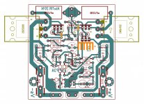
The wide spaced Power and the separated Power Ground are not so good.
Hi Andrew, to which lay-out refers to this?
Many thanks!

Member
Joined 2009
Paid Member
The wide spaced Power and the separated Power Ground are not so good.
You already have separated the power ground and signal ground so you could move the power ground closer to the speaker output at the back edge of the board (left version) and run a trace around the top edges and corners - to make space to bring the traces down the outside edges to the rail caps you will have to move the output power resistors closer together but you have space for that if you nudge things around.
You have space for larger rail caps, or two pairs.
Last edited:
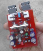
Finally my P3A sung loud & clear 
After about 2hrs of playing, DC offset settled at 02.4dcmv. AC at the output is dead flat at 00.0v (when no signal applied). Very silent too, no humming issues.
Since my PSU was at +-27vdc, I used BC550C for the input diff. MJE15032/33 for drivers 2SA1209 for VAS and 2SC5200/SA1943 for the output. Everything works well no overheating problem.
The lay-out was a success, I could say, I now possess two wonder amps that display remarkable soundstage for a few parts count. (VSSA & P3A)
Many thanks to Ian Finch, Bigun and AndrewT for their inputs.
Attachments
- Home
- Amplifiers
- Solid State
- Rod Elliot P3A Layout - Critics