Two transformers 15W (2х12V, 0.55A) will be enough?
More than enough, sure.
Can I use a single transformer 40W (2x12V, 1.5A) and rectifier circuit in the picture?
Half wave rectifier. Not really ideal. Better to use full wave rectifier and power both boards from the common output.
I have DC voltage (0.015V and 0.01V) at amplifier output. It is within the norm?
Yep. This is excellent, actually.
OPA134PA has Offset Trim. This adjustment will work?
There is no need to trim, but yes, if you want to add the external components and connections needed, you can do it. There's some posts from disfunctionalshadow (I think it was) somewhere down in this thread where he does exactly this.
PS/aside: 1000 posts in the Sapphire amp thread? Wow. I guess I've been hammering away at this for that long, hey?
Last edited:
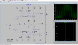
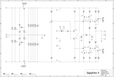
Sapphire 4 [Unity H]
The next iteration of the Sapphire headphone amplifier is a part of Project Unity. It's going in a different direction than the Sapphire 3, and as such the older version will remain current for the foreseeable future.
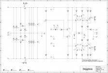
Sapphire 4 aka Unity H drops the voltage regulator from the boards and replaces the op amp with a discrete current feedback amplifier. The parallel output transistors are replaced by a single pair of BD139/140 [Q19,20 in the schema below, which are modeled as BC327,327].
Boards will be unveiled shortly. For the moment, here's the basic circuit;
The next iteration of the Sapphire headphone amplifier is a part of Project Unity. It's going in a different direction than the Sapphire 3, and as such the older version will remain current for the foreseeable future.
Sapphire 4 aka Unity H drops the voltage regulator from the boards and replaces the op amp with a discrete current feedback amplifier. The parallel output transistors are replaced by a single pair of BD139/140 [Q19,20 in the schema below, which are modeled as BC327,327].
Boards will be unveiled shortly. For the moment, here's the basic circuit;
Attachments
Last edited:
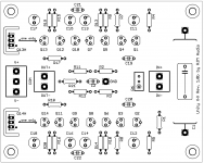
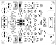
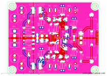
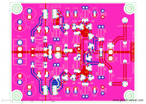
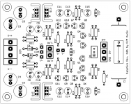
Boards done.
The idea is the boards are dual-purpose. The headphone amp version changes a few resistors and uses the larger TO-126 transistor Q13H and Q14H with a small heatsink rather than TO-92 Q13,Q14. It runs at 50 mA bias.
The gain is adjustable by setting R2,R3. Gains from 3 dB to 20 dB should be do-able, and possibly 30 dB with a couple of tweaks. I'll do up a table in the BOM showing what values to use for the desired gain setting.
The voltage regulator is separate. This one should work nicely.
Attachments
Last edited:
Boards done.
I'm in.
Any provision for upping the quiescent in the TO-126 pair? Would that require a bigger Q11-Q12 pair? If so, forget I asked.
Please post back when things are ready to go.
How much do you need?
The ratio of R11/R17 controls the current multiple, so its just limited by the need to heatsink the transistors and supplying sufficient current to drive them. 100 mA or even 200 mA can be set just by changing a couple of resistors. Device dissipation climbs to 1 W and 2 W respectively. The output transistors can be folded back and screwed down to the chassis or metal block, either vertically or horizontally, for better cooling.
The ratio of R11/R17 controls the current multiple, so its just limited by the need to heatsink the transistors and supplying sufficient current to drive them. 100 mA or even 200 mA can be set just by changing a couple of resistors. Device dissipation climbs to 1 W and 2 W respectively. The output transistors can be folded back and screwed down to the chassis or metal block, either vertically or horizontally, for better cooling.
How much do you need?
How much do I need? Probably no more than the design calls for. How much do I want? Well, now...
It "would be nice" would be to run the output stage in class A. Based on what I've read the consensus seems to be 100ma, give or take. I'm not quite sure how that is arrived at, and (as with all things) is open for discussion. My head tells me that because of the low voltage/current involved in a headphone amp an AB output stage probably stays in class A most of the time, but my heart says not just no but heck no, give me pure class A all the time. To keep ying and yang balanced, I'd say class A if it's reasonable.
At the specified 50 mA the output stage is expected to remain in class A with a considerable margin of safety.
But it all depends on how sensitive the headphones are, what the impedance is, and how loud you want to go.
For your info, my design specification for this is 15 mW minimum class A output 16-300 ohms. This requires a minimum bias current of 28 mA and voltage rails of +/- 6 V and will bring a set of headphones with a typical sensitivity of 95 mW/dB to at least 107 dB. For 60 ohm headphones the output stage delivers 60 mW and 112 dB.
I'd recommend proving to yourself you actually do use more before making changes, you might be surprised to learn you never actually crack 1 mW.
Attachments
Last edited:
For your info, my design specification for this is 15 mW minimum class A output 16-300 ohms. This requires a minimum bias current of 28 mA and voltage rails of +/- 6 V and will bring a set of headphones with a typical sensitivity of 95 mW/dB to at least 107 dB. For 60 ohm headphones the output stage delivers 60 mW and 112 dB
My favorites are Denon D2000s, 25R, 106dB/mW, 1800mW max input. With 15mW min across 16-300R seems like plenty to drive 25R well over 106dB, and I'm not interested in that. At all.
I think I've created much ado about nothing.
No, JFETs are out of the picture as the circuit needs the precise emitter-base pn diode reference voltage of the BJTs to correctly set and stabilize the bias currents throughout the rest of the circuit.
****
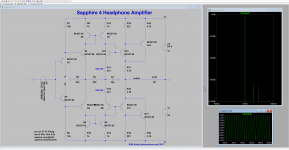
Working/prototype BOM attached. (Unity 1.0e)
****
Working/prototype BOM attached. (Unity 1.0e)
Attachments
Please see the blog post for the most recent BOM. There are a couple of edits from the version posted above.
The boards are on order. I should have them mid-January.
The boards are on order. I should have them mid-January.
or...
we could just go back to a simple drop-in replacement for the older boards, with the regulator built in.
I like this, since it means I can listen to the new version with minimal fuss.
we could just go back to a simple drop-in replacement for the older boards, with the regulator built in.
I like this, since it means I can listen to the new version with minimal fuss.
Attachments
or...
... a simple drop-in replacement for the older boards, with the regulator built in.
I like this, since it means I can listen to the new version with minimal fuss.
I like the sound of that, too!
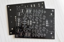
Glad to hear that because I've gone ahead with this version! (4.0b)
Here's all the info. (For download: Gerbers, LTSpice, and BOM)
Here's all the info. (For download: Gerbers, LTSpice, and BOM)
Attachments

Last edited:
BOM revision 4.0b2
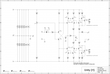
I made some adjustments to the resistance values of the output stage to lower the output impedance a bit. It's about 3 ohms now, vs 7 ohms for the b1 configuration.
R11,12 465 ohms -> 221 ohms
R17-20 10 ohms -> 4.7 ohms
R1 is made 1k, though this is a rather arbitrary value.
R2, R3 and C2 - the gain setting components - have been adjusted slightly. Please refer to the table in the BOM Gain Calculator page. The defaults are now 2k2, 22k, and 10pF respectively. Since this is a current feedback circuit, these components are somewhat of a pain to finesse, but the simulation can be helpful to understand the relationships. Reducing R2 cranks up the open loop gain. This is required to obtain useful bandwidth at high closed loop gain (i.e. circuit gain), but is relatively unstable so a higher value of C2 is needed for compensation. For low closed loop gain R2 can be relaxed since there is plenty of available bandwidth. Less compensation is required here. The closed loop gain is approximately R3/R2 though it is slightly more complex than that in reality especially for high values of R3.
Attachments
Last edited:
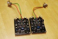
Did the smoke / operating point test.
One board is perfect, the other had -2 V offset that fell out of the range of the trimmer R6. I found the problem was the Zener diodes, which were not well matched so the positive and negative rails were 0.25 V different. If R6 is 1k that only gives 0.1 V of adjustment, not enough to compensate.
This can be solved by matching the Zeners to closer tolerance, but the basic failure here is R6 was too small a value. Increasing R6 to 5k allows about 0.5 V adjustment, which should cover just about any eventuality. You can use 10k if you want.
Since I don't have any 5k trimmers on hand, I'll match some Zeners tomorrow and replace the oddball.
In point of fact I matched the transistors well enough that the trimmer is hardly needed, removing it would actually improve the situation in this instance since the offset is introduced into the input by the power supply through the trimmer itself.
Attachments
Last edited:
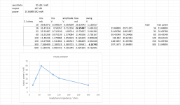
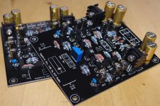
Bench notes, DC operation:
My roll of "12V" Zeners seem to come in two flavors of breakdown voltage. Of seven tested, three were 11.5~11.6 V, while four were 11.2~11.3 V. Odd but that's what I have to work with.
Using one of each type for D1,2 means |(V+) - (V-)|= 300 mV and the center of the trim pot moves 150 mV away from zero. For a 1k pot as R6, the adjustment range is 100<->200 mV i.e. insufficient as zero is out of the trim range. For a 5k pot the range is -100<->400 mV, which is ok.
To fix my board though all I had to do was swap out the 11.6 V D2 Zener for an 11.3 V one to match D1. Now 0 mV it is in range of the 1k trim. In my case it was easier to match Zeners than order a new trim pot, but as I mentioned last post the BOM is updated to increase R6 to 5k.
The output offset of both boards (configured for 26 dB gain with R2 = 475R and R3 = 22k1) after trimming is +/-50 mV cold and +/-10 mV warmed up. The trim setting is so close to zero though it is unclear if the offset adjustment is even needed. If 50-100 mV output offset voltage is acceptable it can probably be left out in favor of a simple 47k resistor to ground, but ultimately its probably safer to keep the trim option.
The bias current is about 40 mA, and the heatsinks barely get warm to the touch, so there is plenty of thermal headroom if higher bias currents are desired. This is accomplished by increasing R11,12 from 221 ohms to 332 ohms or even 475 ohms.
Attachments

Last edited:
- Home
- Amplifiers
- Headphone Systems
- RJM Audio Sapphire Desktop Headphone Amplifier