like nothing else I've heard
A phrase sadly worn out from overuse but I can't help but agree with you absolutely. Hopefully just this once I'll be forgiven for talking up my own work: It honest, legit completely up-ended my previous conception of what headphones and headphone amplifiers were capable of.
P.S. Thanks again, Mike, for the files.
My Sapphire 4 build employs .68uF input coupling caps and the lower bass coming through my DT880's is marvellous: natural, clean, airy, and revealing recording space like nothing else I've heard.
What brand and model of .68uF caps are you using or prefer?
Thanks.
What brand and model of .68uF caps are you using or prefer?
Thanks.
I'm using ClarityCap MR.
My Takman pot is getting old
Stiff, notchy and static on the detents. I'm thinking about buying one of those Goldpoint V24 attenuators. I think you installed a 25K unit, Richard?
The current BOM says 20K, does it matter? 25K or 20K? These things cost enough, I want to buy the right one!
Stiff, notchy and static on the detents. I'm thinking about buying one of those Goldpoint V24 attenuators. I think you installed a 25K unit, Richard?
The current BOM says 20K, does it matter? 25K or 20K? These things cost enough, I want to buy the right one!
Last edited:
like nothing else I've heard
A phrase sadly worn out from overuse ...
Yes, indeed. Nevertheless, a true statement.
Stiff, notchy and static on the detents. I'm thinking about buying one of those Goldpoint V24 attenuators. I think you installed a 25K unit, Richard?
The current BOM says 20K, does it matter? 25K or 20K? These things cost enough, I want to buy the right one!
10-50k is fine. -> RJM mentioned in BOM
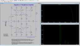
I borrowed the BD139,140 models Mike used in his LTSpice simulation. BD135,137,139 and BD136,138,140 are the same but for the voltage rating.
Changing the output transistor from BC337/327 to BD139/140 has no material influence on the simulation output that I could see.
One of the more useful things you can do with the sim is compare open loop and closed loop distortion for different values of R2,R3(X). You can also remove R3(X) and look at the open loop gain and phase margin as a function of R2.
Attachments
About making comparisons in simulations, I would recommend trying out the free version of SIMetrix. Has a unique function that does not have any other simulation software: it can accumulate several curves in a same graph. That is, when a variable is changed and a new simulation is made, a new graph is not generated, but each new curve is represented in the same graph, which makes the comparisons extraordinarily easy. Very useful:
https://www.simetrix.co.uk/downloads/download-elements.html
https://www.simetrix.co.uk/downloads/download-elements.html
I'm sorry, he's the only one who has that function.
Maxim EE-Sim is also based on SIMetrix, perhaps it allows more components:
http://maxim.transim.com/Loader/Downloads.aspx
Maxim EE-Sim is also based on SIMetrix, perhaps it allows more components:
http://maxim.transim.com/Loader/Downloads.aspx
Last edited:
One of the more useful things you can do with the sim is compare open loop and closed loop distortion for different values of R2,R3(X). You can also remove R3(X) and look at the open loop gain and phase margin as a function of R2.
How did you manage the 2nd graph, the one that shows the harmonic components? It has to be a graph of the FFT values. I've been unable to find the magic incantation for that.
First you set the input signal to generate a sinewave, and plot the output signal you want to measure the FFT of. Then you right-click on the sine wave plot, select view->FFT.
Outstanding! I asked that question in the sw tools forum, but didn't get a response. The more I play with the tool, the more I learn, the more I like.
The THD values are much more revealing with a graph. I've not yet had a chance to really explore, but the THD seems to be lower when the buffer is not in the feedback loop? I didn't change any values, just move the connection. But I also think I recall that yours is configured to include the buffer stage, that was your preference. I'll have to listen to both when the build is complete.
I also didn't realize that R2 affects open-loop gain. With R2 approx 2K and R3 approx 4K total gain is 6dB, with R3 removed it's 54dB (give or take). Giving around 48dB closed loop gain. I have the impression there is a school of thought that lower closed loop gain is "better"? Another research topic, I like those.
So regarding R2 and R3(X) and distortion ... it's complicated.
R2 sets the open loop gain. Give yourself a pat of the back for figuring that one out, as that's the key entry point to all this CFA business. The trick is though, you cannot, for various reasons, make R2 arbitrarily small.
The next thing to notice is that using the same resistor value for R3 and R3X actually gives different circuit gain. There is 6 dB (2x) difference, with R3X giving higher gain. So in this instance the distortion simulation will indicate that R3X connection has higher distortion, but this is correct: you haven't changed the open loop gain since R2 is the same, but you've increased the gain so there is less feedback applied, so of course distortion increases.
The important thing to understand is that driving the feedback via R3 and therefore Q9,10 is sub-optimal because that node has no more current drive than Q3,Q4. So the resistance R3 has to be large, and, for a given gain, R2 has to be large also: and as a result there is less open loop gain than you'd ideally want especially for low gain settings. Connecting with R3X gives you access to the enormous current reserves of that big, powerful buffer to drive the feedback loop, so R2 and R3 can be made as small as you want. Except that now you're facing a different problem, namely phase shift. R2 too small, bandwidth too high, phase margin too small, circuit becomes unstable.
With R3X though, at least you are no longer limited by the current drive of Q9,10 and you are free to make R2 as small as you dare given stability concerns, this is why you'll see that the R3X connection (with the BOM values) give better performance than the R3 connection (with BOM values). The reduction in distortion for a given gain setting scales almost exactly with the change in R2.
Last edited:
That was the electrical engineering story. The takehome for audiophiles is as follows:
R3: buffer open loop, more distortion but predominently 2nd harmonic so overall pleasing character, low bandwidth so possibility of operational instability essentially nil and possibility of RFI and similar HF problems also nil.
R3X: buffer in feedback loop, overall lower distortion but 2nd harmonic is preferentially reduced leaving more higher order components, bandwidth in excess of 1 MHz so proper bypassing and shielding are more of a concern, instability a significant risk meaning care must be taken choosing the resistance values R2,3X.
Last edited:
Transistor specs
I'm considering buying new transistors at a higher spec so that Q1 and Q2, as well as the downstream pairs, can be better matched in Hfe than I was able to achieve with the spec I bought for the prototype 4.0b boards. So, instead of BC33725BU, I'd get BC33740TA (the bulk BU spec is n/a). Similarly for BC327.
These 40-spec transistors have considerably higher Hfe, but I can match them, something I was unable to do the the 25-spec 327 and 337.
Or will higher Hfe cause problems? Is there a reason you haven't specified the higher grade in 4.1m?
Goldpoint, btw, is basically reselling an ELMA unit. I don't know what the exact details of the arrangement are, and since the Elma-sourced part isn't significantly cheaper (if it is available through consumer channels at all...) it doesn't really matter.
Attachments
Last edited:
Three grades of BC327/337 are sold, binned by hfe: -16 is 100-250, -25 is 160-400, and -40 is 250-630.
As far as the Sapphire circuit goes, the hfe of the transistors doesn't make a huge difference, chiefly through Q1,Q2, where higher hfe improves both the input impedance and PSRR.
Generally speaking higher is better, but as you see the -40 grade has a wider spread of values, so there will me more scatter of the individual devices in a typical build, and this could - I imagine, I haven't examined it in detail - increase distortion.
I picked -25 grade as being a compromise. If you want to use -40 and bin the devices yourself to tighter tolerances go ahead ... just be aware you won't get that much back for your trouble.
Given the wider spread I guess you are right and it will be more likely to find matched pairs of -40 grade parts. Here again I'm not sure if the reward will be worth the effort but it is an ingenious idea.
Attachments
Last edited:
- Home
- Amplifiers
- Headphone Systems
- RJM Audio Sapphire Desktop Headphone Amplifier