Accusilicon are not expensive IMHO, but even if they are to some folks so are some of the parts Marcel uses for the dac board, at least the cost adds up in aggregate. Regarding my clock board, if I share it then I will share the KiCad project. Then if people want to change it they can.
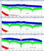
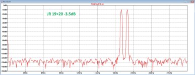
Surprised by the spectrum of the JRiver converted 0dB@1Khz PCM file having no Spectral lines around fs/2 and 3fs/2, I also inspected a -60dB@1Khz file and a 19Khz + 20Khz at -3.5dB peak both PCM files also converted by JRiver.
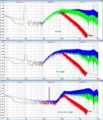
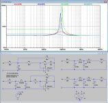
Blue is input to the shift-register, Green is at the Firdac's summing point and Red is the output from the 80Khz reconstruction filter as shown in last attachmment.
Also for these situations there are no signs of spectral lines at fs/2 and 3fs/2.
Marcel, is this because of the use of a quasi multi bit conversion.?
Finally I added in the third attachment the spectrum up to 30Khz processed by the 5th order filter with added OPA1632, having 13.3dB gain to get the required 2Vrms@0dB.
No obvious signs of IM are visible for as far the OPA1632 is accurate in showing distortion.
Arta recorded image below shows the measurement from the original Firdac below with the very same .dsf file.
Hans
Attachments
Quick sim confirms FR is nice and noise gain seems to be manageable (but still quite high, 25dB), but input impedance doesn't look that good with 70R at 20kHz. I don't know what the "original filter design" was, though (can seem to find it right now).It is roughly a fourth-order Butterworth filter at 80 kHz. Up to 20 kHz, its input impedance is not much worse than that of the original filter.
The original filter's virtual ground isn't that great either. In fact, it's theoretically 481.2951 uH in parallel with 198.1796358 ohm (DAC resistance not included) in parallel with 8.2 nF per side. The inductance dominates at 20 kHz, leading to an impedance of about 60 ohm per side, 120 ohm differential. The peak around 80 kHz is better damped in the original filter, though.
Last edited:
Marcel, is this because of the use of a quasi multi bit conversion.?
I don't know, they might also have found a very effective dithering scheme.
For large signals, there are very many very small FM components, so small you probably wouldn't notice them. It is interesting that you also don't see any at -60 dBFS, 1 kHz.
Accusilicon are not expensive IMHO, but even if they are to some folks so are some of the parts Marcel uses for the dac board, at least the cost adds up in aggregate. Regarding my clock board, if I share it then I will share the KiCad project. Then if people want to change it they can.
Hi Mark ... well, I reckon you already have seen this datasheet but just in case you have not I have attached a copy of the NZ2520SDA oscillator datasheet with phase noise plots (at the end of the datasheet). It seems to me that they have identical specs at the lower offset frequency range and actually is a little bit better at the higher offset ranges (e.g. 1MHz, 49 MHz) than the AS318BM series. And they are available at e.g. Digikey at a very reasonable price ...
Just intended to be a slight digression but might I ask why you would choose the Accusilicon over the NZ2520SDA?
Cheers, Jesper
Last edited:
U
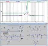
1) The original filter viewed that way has a very nice almost flat impedance within a small band, see Red trace below.
2) The filter proposed in your recent posting in Blue, has a rather large peak at 80Khz, when the design was understood correctly
3) The 5th order passive filter in Green has an even higher peak and rather disqualifies for the purpose when opting for a flat impedance versus frequency.
4) The 4th order passive filter in Teal, terminated with 210R, has a nice flat 590R impedance up to almost 80Khz and goes to 380R upwards from 100Khz.
This version has a 3dB lower output as a version with 380R termination, but even then, the noise from the amp (OPA1632 ?) behind the filter will still be quite a bit lower
Hans
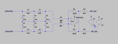
Marcel, when it's O.K. to look at the filter from a point of view, that for the design of the filter all shiftregisters can be replaced by one voltage source with a 380R in series, then the impedance for different (Butterworth) filters comes out as follows:Regarding filters, what I would like to try is a differential version of something like this:
View attachment 1300098
where N1 is a nullator (ideal op-amp input port) and NR1 a norator (ideal op-amp output port) that have to be replaced with some discrete amplifier circuit I haven't designed yet. It needs to have a low equivalent input noise voltage because of the effect of C2 on its noise gain.
It is roughly a fourth-order Butterworth filter at 80 kHz. Up to 20 kHz, its input impedance is not much worse than that of the original filter.
1) The original filter viewed that way has a very nice almost flat impedance within a small band, see Red trace below.
2) The filter proposed in your recent posting in Blue, has a rather large peak at 80Khz, when the design was understood correctly
3) The 5th order passive filter in Green has an even higher peak and rather disqualifies for the purpose when opting for a flat impedance versus frequency.
4) The 4th order passive filter in Teal, terminated with 210R, has a nice flat 590R impedance up to almost 80Khz and goes to 380R upwards from 100Khz.
This version has a 3dB lower output as a version with 380R termination, but even then, the noise from the amp (OPA1632 ?) behind the filter will still be quite a bit lower
Hans
Attachments
As many here are already using PCM2DSD with fixed DSD256 output the need to support larger range of DSD rates is probably not that important.If you want to support a large range of DSD rates and always have notches at multiples of half the sample rate, you either need a whole bunch of crystals, or have to accept frequency dividers, or use a much longer FIRDAC.
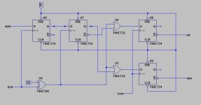
Regarding "crystal clocking" this is what it looks like simplified. As BCK & SD is typically generated from MCK upstream there probably already exists some timing offset so RC delays may not be needed but series termination resistors should probably be added to input & output lines to cater for timing tuning.
Couple of questions:
Is it correct to assume that with this scheme BCK is no longer critical for low noise but instead MCK is?
Is U4 (XOR) needed?
Attachments
I just noticed that the mentioned 210R termination in #2868 was 50R instead.
It should have been 210R, here is the correct attachment.
1) The original filter has a very nice almost flat impedance within a small band, see Red trace below.
2) The filter proposed in your recent posting in Blue, has a rather large peak at 80Khz, when the design was understood correctly
3) The 5th order passive filter in Green has an even higher peak and rather disqualifies for the purpose when opting for a flat impedance versus frequency.
4) The 4th order passive filter in Teal, terminated with 210R, has a nice flat 590R impedance up to almost 80Khz and goes to 380R upwards from 100Khz.
This version has a 3dB lower output as a version with 380R termination, but even then, the noise from the amp (OPA1632 ?) behind the filter will still be quite a bit lower
Hans
Attachments
Hi Jesper,Oooups .. forgot the attachment ... here it is:
Don't want to get into a big diversion in this thread but I will say that IMHO phase noise plots are to some extent analogous to FFT plots. Neither one is fully predictive of how something will sound. Neither one contains complete information either. For FFTs its phase information that is usually missing. For Phase noise plots, we can only approximate RMS time domain jitter from phase noise. And I'm not sure that RMS jitter is good enough anyway. For example, RMS voltage is not directly convertible to peak voltage unless we know the time-domain waveform to begin with.
Anyway in what I would call the consumer grade of clocks I have tried, they are NDK SDA, Crystek, and Accusilicon. For NDK SDA in particular, I have tried ones from Jocko Homo that measure among the best NDK makes (about the top 10% of NDK production based on phase noise measurements were the ones Jocko sold as the best available). What I have found is that NDK SDA usually sounded the worst of the three consumer types just mentioned. Accusilicon maybe sound the best. This was with a variety of power supplies and clock loads which were tried over time. In addition, Andrea Mori told me he would use Accusilicon if he had to choose among the three consumer grade clocks.
So, that's it for me. I will use TH Pads and or sockets compatible with Accusilicon. If someone wants to use NDK SDA they can make an adapter board, or modify the clock board KiCad files. One thing I don't want to do is make universal pads to accommodate any clock. I don't think those layouts including the bypass caps are ever optimal, and they just encourage using the cheapest clocks based on measurements that don't tell everything about how a clock will sound. Now, would all the clocks sound the same on my clock board because I baby the clocks as much as I can? Maybe, but I've spent about as much time on the clock board as I want to, so I will go with with I think is most likely to work well.
Mark
Last edited:
One thing I might suggest would be get notification if these ever become available again: https://www.digikey.com/en/products...AZU4BOASwB2AcxABfIgFoAHEhCpImXIRLlwYOQE5Wkg0A
They might make the cost of the clock board more palatable, and also leave plenty of caps for other projects. Price of the kit is steal, IMHO.
Also, each board will use two of: https://www.mouser.com/ProductDetail/863-NC7SZ74K8XL22236 ...which are EOL. IIUC drop-in parts are available in LVC but the NC7SZxxxx parts may be better.
Last edited:
I just noticed that the mentioned 210R termination in #2868 was 50R instead.
It should have been 210R, here is the correct attachment.
1) The original filter has a very nice almost flat impedance within a small band, see Red trace below.
2) The filter proposed in your recent posting in Blue, has a rather large peak at 80Khz, when the design was understood correctly
3) The 5th order passive filter in Green has an even higher peak and rather disqualifies for the purpose when opting for a flat impedance versus frequency.
4) The 4th order passive filter in Teal, terminated with 210R, has a nice flat 590R impedance up to almost 80Khz and goes to 380R upwards from 100Khz.
This version has a 3dB lower output as a version with 380R termination, but even then, the noise from the amp (OPA1632 ?) behind the filter will still be quite a bit lower
Hans
Hi Hans,
On one hand, I would like to keep the signal voltages at the FIRDAC summing nodes as small as possible because they make the current drawn from the reference data-dependent. On the other hand, I don't see how you could keep the impedance there really low while still having substantial passive filtering before you reach the first active device of the analogue output filter.
As you can see in your own simulations by subtracting the source impedance, the red and blue traces have the lowest impedance at the summing node over the frequency range traditionally considered audible for humans (*), but I don't know if that is the right criterion. It helps to keep the summing node signal swings (and hence any artefacts those may cause) small when it is mostly audio causing those swings, like when you listen to loud passages. During near silence, it is mostly the shaped quantization noise causing swings. The blue trace indeed has a rather nasty peak around its cut-off frequency.
By definition, a lossless LC filter passes all power the signal source delivers to its input on to its load (it has to, as it's lossless). It can therefore only suppress signals in the stopband by changing its input impedance such that the signal source can't deliver much power to it anymore. For a filter working between two equal resistive terminations, you have the maximum power transfer when the filter input impedance equals its load resistance, and a change of the filter input impedance in any direction (up, down, or added positive or negative reactance) reduces the transfer.
In its passband, a lossless LC ladder filter normally has an input impedance essentially equal to its terminating resistance. For example, in a low-pass filter with inductors as series and capacitors as shunt branches, the whole filter becomes one big short between source and load when the frequency goes to zero.
I suspect that lossless LC filters designed to work between a current source and a resistive load will tend to have an input impedance that drops to zero in their stopband. The real part of the input impedance will definitely have to drop, as that is the only way the filter can reduce the power I2Re(Zin) delivered by the current source.
So maybe the best approach would be an LC ladder filter designed for an infinite source and low load resistance (or one designed for a high source resistance and low load resistance having component values close to those of a filter designed for an infinite source and low load resistance). I don't agree with your remark about 3 dB less signal, as the current through the load resistance only goes up, and both in your and my proposal, the stage after the LC filter essentially looks at the current rather than the voltage. The values of the filter capacitors will increase as the load resistance is reduced, this will eventually cause an excessive noise gain for the stage after the LC filter. The required values of the inductors go down, leading to higher self-resonance frequencies and possibly less inductor distortion at a given current and core size. I don't know yet whether there is some way to intertwine this with an MFB stage without getting nasty impedance peaks.
Thanks Hans, I think I have a better idea about what I'm trying to do now.
Regards,
Marcel
(*): Cats can hear some two octaves more, but despite their superior hearing, they are usually less fussy about sound quality.
Last edited:
Couple of questions:
Is it correct to assume that with this scheme BCK is no longer critical for low noise but instead MCK is?
Yes, if it is also MCK driving the shift registers. The MCK frequency has to be twice the BCK frequency to get the FIRDAC notches at the right places.
Is U4 (XOR) needed?
No idea, it depends on the unspecified timing relation between BCK and MCK. You can kick out U4 as well as U7 if you can then still meet all set-up and hold times.
Wasn't one of your design goals with two Firdac shiftregisters working complementary, to get a constant current drawn from Vref ?Hi Hans,
On one hand, I would like to keep the signal voltages at the FIRDAC summing nodes as small as possible because they make the current drawn from the reference data-dependent. On the other hand, I don't see how you could keep the impedance there really low while still having substantial passive filtering before you reach the first active device of the analogue output filter.
Keeping the summing points at a constant voltage can only be achieved by feeding them in an inverting amplifier's virtual ground, but that seems to be a hard task for an amp given the high level ultrasonic HF content , resulting in nasty modulation products for low level signals.
Yes, unless you start the filter with a an inductor and end with a cap, although a virtual input has zero input impedance over the whole FR.I suspect that lossless LC filters designed to work between a current source and a resistive load will tend to have an input impedance that drops to zero in their stopband. The real part of the input impedance will definitely have to drop, as that is the only way the filter can reduce the power I2Re(Zin) delivered by the current source.
Yes true concerning the 3dB, I was looking at it from a voltage perspective without amp behind it, in that case 3dB less signal would be available behind the filter, but connected to the virtual input of an amp, the current increases with a lower termination.So maybe the best approach would be an LC ladder filter designed for an infinite source and low load resistance (or one designed for a high source resistance and low load resistance having component values close to those of a filter designed for an infinite source and low load resistance). I don't agree with your remark about 3 dB less signal, as the current through the load resistance only goes up, and both in your and my proposal, the stage after the LC filter essentially looks at the current rather than the voltage.
Yes, it is finding a difficult compromise between all these conflicting options.The values of the filter capacitors will increase as the load resistance is reduced, this will eventually cause an excessive noise gain for the stage after the LC filter. The required values of the inductors go down, leading to higher self-resonance frequencies and possibly less inductor distortion at a given current and core size. I don't know yet whether there is some way to intertwine this with an MFB stage without getting nasty impedance peaks.
Looking forward to see your next design.Thanks Hans, I think I have a better idea about what I'm trying to do now.
Hans
An article on making audio frequency filters using transformers: https://ka7oei.blogspot.com/2013/01/an-lc-audio-bandpass-filter-using.html
Something like this occurred to me previously, which is to say, thinking about using transformers in filters even if only as simple inductors. Regarding self resonance and effectiveness at RF frequencies, seems to me the transformer/inductors may become usefully lossy at higher RF frequencies.
Something like this occurred to me previously, which is to say, thinking about using transformers in filters even if only as simple inductors. Regarding self resonance and effectiveness at RF frequencies, seems to me the transformer/inductors may become usefully lossy at higher RF frequencies.
@Markw4 :
Thanks for the tip, Mark") (I am familiar with these components) ...
(I am familiar with these components) ...
Cheers, Jesper
One thing I might suggest would be get notification if these ever become available again:
Thanks for the tip, Mark
(I am familiar with these components) ...Cheers, Jesper
Not the ones Cinemag made for Quadratic Audio, nor some prototype line level transformers here (still under NDA unfortunately). IIUC Cestrian is using some Lundhal transformers that may be pretty good. Of course, they may not be low-cost.Don't they distort substantially?
Also, if transformers filter out RF in a way that sounds better than, say, opamps, then they may be more fit for purpose than, again, say, opamps. Just saying if the goal is to satisfy human perception of a very close to real listening experience, PSS distortion is not the only factor that affects the end goal (as Paul Frindle found out).
Last edited:
- Home
- Source & Line
- Digital Line Level
- Return-to-zero shift register FIRDAC