Hi Oliver
Fine, it is not very thick, less than 0,1 um.
Anyway, it should be ok for soldering with non-eutectic solder.
Hi Saulius,
the Immersion Gold thickness of my pcb´s is 1-3 microinch.
Fine, it is not very thick, less than 0,1 um.
Anyway, it should be ok for soldering with non-eutectic solder.
Hi
Having spent the festive break reading through the thread a few times I would like to make the following observations / suggests / questions.
1. If I build the boards (psu / salas shunts / dac) as per the diagrams and BOM then I should have a working DAC.
2. If the I2S source does not have a buffer then I need the new high-speed buffer board (at the moment I am sucessfully running I2s from a QA-550 into Buffalo 32S and from a juli@ into Buffalo II - since neither of these dacs seems to have a buffered input I assume there should not be a problem with the TDA1541A board!!).
3. It would be better to remove the TL431s and associated circuitry; in this case it would seem to be better to chop the board removing the TL431 section and wiring the Salas shunts as close as possible to the TDA1541A - a possible future version of the boards could have 3 parts for the DAC board - input psu connections board / TL431 board / DAC board? The Salas shunt boards could also have the outputs aligned to the DAC board allowing for even shorted connections?
4. Having a v2.3 board I do not have to lift any feet on the 74HC02.
5. Worry about the appropriate IV stage later!
If the above is correct then I will order all the bits (excluding TL431 bits) as per Ryelands excellent spreadsheet and get building.
Regards
Alan
Hi Alan
As you have probably read, I am using the 2xDAC without the TL431s, and to get the Salas shunts as close as possible I have cut my boards in half, and scraped the solder mask off 8mm(ish) of the relevant traces onto which I have soldered 0.6mm silver solid core wires. It is not pretty, but it works perfectly.
I cannot give a sound comparison, as I wasn't fully burnt in when I cut my boards, as I believe strongly in the idea to do it, so just went ahead. I think it was the right thing to do. Voltage regulation is perfect and fully adjustable, and of a much higher quality without the TL431s in my opinion. There is no inter-modulation, of course, and the DAC sounds beautiful. This is a trade off between aesthetics of the finished boards and sound logical circuit design in my opinion. Why take two sets of shunt regs into the shower?
I hope that helps.
Oliver,
Has anybody managed to get the spdif input working on this dac yet? I would love to do that as the USB isn't working for me, as I can't use a long cable on this Teradac, and want to get my Airport Express back up and running.
Many thanks
Lucas
Got it working!
With the missing 74HC125 between the Twisted Pear Opus WM8804 and the DAC modules, it runs like hell.
An externally hosted image should be here but it was not working when we last tested it.
The configuration is as followed
Pin1: to GND
Pin2: Input 1
Pin3: Output 1
Pin4: to GND
Pin5: Input 2
Pin6: Output 2
Pin7: GND
Pin8: Output 3
Pin9: Input 3
Pin10: to GND
Pin11: N.C.
Pin12: N.C.
Pin13: N.C.
Pin14: Vcc (+5V)
Perhaps someone have a nice small DIP14 pcb witch looks better than mine.

Ahah!!!! I see you have got it working.....Most excellent. Good work Herr DeutscheDac.. I will now look into this properly.
Hi Alan
As you have probably read, I am using the 2xDAC without the TL431s, and to get the Salas shunts as close as possible I have cut my boards in half, and scraped the solder mask off 8mm(ish) of the relevant traces onto which I have soldered 0.6mm silver solid core wires. It is not pretty, but it works perfectly.
I'm gonna do the same, go without TL431.
IMHO, big power supply (15 caps in parallel) and Salas shunt regulator is enough for one power line for sure.
My Reference TDA1541A DAC project comes to the final stage, the housing.
After my decision to make a tube rectifier circuit for the B+ of the Tube-I-zator output stage,
i will make a two case design with a separate case for the PSU.
Into the PSU case i will insert the two +/- Power Supply Modules and the Tube rectifier circuit.
The transformer goes on the top of the case in a separate aluminum housing. Also the tube rectifier goes on top.
Because i will use only MKP Mundorf caps in the rectifier circuit, the 47µF and the two 100µF caps goes through the top panel.
(both channels gets their own Salas HV-Shunt module)
Top panel
Front panel
Back panel
Here the tube rectifier circuit
That´s the first step. If i am ready with the build of the PSU, the DAC case is next")
After my decision to make a tube rectifier circuit for the B+ of the Tube-I-zator output stage,
i will make a two case design with a separate case for the PSU.
Into the PSU case i will insert the two +/- Power Supply Modules and the Tube rectifier circuit.
The transformer goes on the top of the case in a separate aluminum housing. Also the tube rectifier goes on top.
Because i will use only MKP Mundorf caps in the rectifier circuit, the 47µF and the two 100µF caps goes through the top panel.
(both channels gets their own Salas HV-Shunt module)
Top panel
An externally hosted image should be here but it was not working when we last tested it.
Front panel
An externally hosted image should be here but it was not working when we last tested it.
Back panel
An externally hosted image should be here but it was not working when we last tested it.
Here the tube rectifier circuit
An externally hosted image should be here but it was not working when we last tested it.
That´s the first step. If i am ready with the build of the PSU, the DAC case is next
Glad to read that you are moving ahead (me, I have to wait for the AE transformer, sometimes I wonder if it worth). Have you done a comparison between solid state and tube rectifier or you are just going to build it anyway ?
There so many tubes to choose from, have you considered 274 (costly, I know) or 5U4G ?
There so many tubes to choose from, have you considered 274 (costly, I know) or 5U4G ?
I know the differences from my previous DAC project
with a 6X4. It's the cherry on the cake
The simulation is for a 5Y3GT. I will use a Mullard CV378 Big Bottle, that i have
(same as on my 300B Mono's). If i hadn't this one, i would use a 6106 or GZ32.
All have a slow start, witch is good for the tubes on the Tube-I-zator
with a 6X4. It's the cherry on the cake
The simulation is for a 5Y3GT. I will use a Mullard CV378 Big Bottle, that i have
(same as on my 300B Mono's). If i hadn't this one, i would use a 6106 or GZ32.
All have a slow start, witch is good for the tubes on the Tube-I-zator
USB to I2S via PCM2706
I am just catching up on this thread. Looks like a great project. In case it is of interest, I have had good results with an alternative for the USB to I2S stage using the PCM2706. I hard wired the output of the PCM2706 right to the TDA1541a with no resistors, buffers or anything in the path. The 2706 is actually Peter Daniel's fine USB DAC kit truncated after the TI chip. It has very good power supplys to each consumer on the 2706 and the clock. Used teflon CATV for the I2S and kept it short. Simple set up that works very nicely.
I am just catching up on this thread. Looks like a great project. In case it is of interest, I have had good results with an alternative for the USB to I2S stage using the PCM2706. I hard wired the output of the PCM2706 right to the TDA1541a with no resistors, buffers or anything in the path. The 2706 is actually Peter Daniel's fine USB DAC kit truncated after the TI chip. It has very good power supplys to each consumer on the 2706 and the clock. Used teflon CATV for the I2S and kept it short. Simple set up that works very nicely.
I am just catching up on this thread. Looks like a great project. In case it is of interest, I have had good results with an alternative for the USB to I2S stage using the PCM2706.
I hard wired the output of the PCM2706 right to the TDA1541a with no resistors, buffers or anything in the path.
The PCM2706 is also running internally on 3.3V as the most other USB to I2S converter devices.
If you want to use my Reference-DAC module, see the advice of post #407.

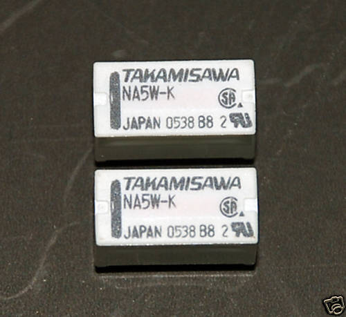
I2S Switch
Because i don´t found a really good solution to switch two I2S inputs
(e.g. USB & SPDIF), i´ve designed the following module:
If there is some interest, i could produce some more.
Because i don´t found a really good solution to switch two I2S inputs
(e.g. USB & SPDIF), i´ve designed the following module:
An externally hosted image should be here but it was not working when we last tested it.
An externally hosted image should be here but it was not working when we last tested it.
- separate relays for each I2S signal to get the maximum HF-Isolation
- based on the Takamisawa NA-5WK relay, witch has minimal HF-Insertion loss
- two layer design
If there is some interest, i could produce some more.
Attachments
Last edited:
I would certainly love one of those relay boards, if you have one going Oliver. As you may know, I am still USB only, but for years I had my Airport Express zapping the digital signal to my optical port on my old dac, and it freed up my music listening and made it a pleasure. Now, I have a USB dac that sounds fantastic, but to use it I have to put my laptop within 1 metre of it, as it doesn't work with longer cables - this sucks for me, so I want an optical input soon, and you have (quite brilliantly) provided the solution.
It would be great if there was provided with the i2s buffer option, I just hate the extra cables going from source to relays then to buffer and then to tda1541 board.
If there is too much hassle Oliver to make this option you could make this board same size with i2s buffer and put header pins of some kind so they could share the same voltage input and the output of the buffer goes the input of the relay board
If there is too much hassle Oliver to make this option you could make this board same size with i2s buffer and put header pins of some kind so they could share the same voltage input and the output of the buffer goes the input of the relay board
Because i don´t found a really good solution to switch two I2S inputs
(e.g. USB & SPDIF), i´ve designed the following module:
An externally hosted image should be here but it was not working when we last tested it.
An externally hosted image should be here but it was not working when we last tested it.
- separate relays for each I2S signal to get the maximum HF-Isolation
- based on the Takamisawa NA-5WK relay, witch has minimal HF-Insertion loss
- two layer design
If there is some interest, i could produce some more.
Oliver
This is the relay that you mean right...????

"Reference" TDA1541A DAC project module summary
Here are the main modules
+/- Power Supply Module
- up to 15 caps per rail (16mm to 18mm diameter)
- place for decoupling foil cap in each rail
- place for bleeder resistor
- 105µm copper weight
- 2mm pcb
- Immersion Gold
- green soldermask on both side
- Board size 195mm x 120mm
Shunt regulator modules
circuit design by Salas
- Shunt regulator module for TDA1541A (+5V, -5V, -15V)
- separate Shunt regulator module for additional parts (+5V)
- 70µm copper weight
- 2mm pcb
- Immersion Gold
- green soldermask on both side
- Board size 147mm x 115mm (46mm x 115mm; single +5V)
TDA1541A DAC Module
- separate TL431 Shunt regulators for each voltage line
- independent voltage rail for the DEM reclock circuit
- I2S attenuator circuit
- shortest possible position for decoupling caps
- separate ground line for decoupling caps
- Ground plane
- 2mm pcb
- Immersion Gold
- green soldermask on both side
- 35µm copper weight
- Board size 125mm x 125mm
The prices are:
+/- Power Supply Module: $23
TDA1541A shunt regulator Module: $20
Shunt regulator Module for add. +5V line: $10
TDA1541A DAC Module: $18
Worldwide shipping: $ 9
Europe shipping: $ 5
paypal fee: 3,9%
The prices for these modules will include a donation of $3 USD to diyAudio for every pcb sold.
Here are the Upgrade modules
With small modifications on the +5V Shunt Reg. Module,
you could use it also for +3,3V output voltages.
For those who are interested in the much faster NL17SZ02,
you could order my 74HC02 - NL17SZ02 adapter pcb.
It will be shipped "ready to use" with the NL17SZ02 chip soldered.
The price for it is $7,50
Worldwide shipping: $ 4
paypal fee: 3,9%
The Ultra High Speed Buffer Module will be shipped "ready to use",
with three NC7SZ125 chips soldered.
Description
Most I2S converter typical supply voltage equals 3.3V.
The I2S attenuators from ecdesigns i am using on my DAC module, are designed for 5V TTL levels only.
So we need the buffer between the output of these 3.3V devices and the input of my DAC module
for a proper work, without canceling the advantages of the I2S attenuators.
- 2mm pcb
- Immersion Gold
- green soldermask on both side
- 35µm copper weight
- Board size 50mm x 42mm
The price for it is $11
Worldwide shipping: $ 4
paypal fee: 3,9%
The I2S switch module (e.g. USB & SPDIF).
- separate relays for each I2S signal to get the maximum HF-Isolation
- based on the Takamisawa NA-5WK relay, witch has minimal HF-Insertion loss
- 2mm pcb
- Immersion Gold
- green soldermask on both side
- 35µm copper weight
- Board size 45mm x 35mm
The price for it is $8
Worldwide shipping: $ 4
paypal fee: 3,9%
At last the Star Grounding Scheme of my complete project.
In the attached files you find the revised BOM from Ryelands including all parts cost in USD
and the technical data for the Takamisawa NA type relays.
Oliver
For a better overview of my whole project,
i think it´s time to make a module summary in one post.
i think it´s time to make a module summary in one post.
Here are the main modules
+/- Power Supply Module
An externally hosted image should be here but it was not working when we last tested it.
An externally hosted image should be here but it was not working when we last tested it.
- up to 15 caps per rail (16mm to 18mm diameter)
- place for decoupling foil cap in each rail
- place for bleeder resistor
- 105µm copper weight
- 2mm pcb
- Immersion Gold
- green soldermask on both side
- Board size 195mm x 120mm
Shunt regulator modules
circuit design by Salas
An externally hosted image should be here but it was not working when we last tested it.
An externally hosted image should be here but it was not working when we last tested it.
- Shunt regulator module for TDA1541A (+5V, -5V, -15V)
- separate Shunt regulator module for additional parts (+5V)
- 70µm copper weight
- 2mm pcb
- Immersion Gold
- green soldermask on both side
- Board size 147mm x 115mm (46mm x 115mm; single +5V)
TDA1541A DAC Module
An externally hosted image should be here but it was not working when we last tested it.
An externally hosted image should be here but it was not working when we last tested it.
- separate TL431 Shunt regulators for each voltage line
- independent voltage rail for the DEM reclock circuit
- I2S attenuator circuit
- shortest possible position for decoupling caps
- separate ground line for decoupling caps
- Ground plane
- 2mm pcb
- Immersion Gold
- green soldermask on both side
- 35µm copper weight
- Board size 125mm x 125mm
The prices are:
+/- Power Supply Module: $23
TDA1541A shunt regulator Module: $20
Shunt regulator Module for add. +5V line: $10
TDA1541A DAC Module: $18
Worldwide shipping: $ 9
Europe shipping: $ 5
paypal fee: 3,9%
The prices for these modules will include a donation of $3 USD to diyAudio for every pcb sold.
Here are the Upgrade modules
With small modifications on the +5V Shunt Reg. Module,
you could use it also for +3,3V output voltages.
An externally hosted image should be here but it was not working when we last tested it.
For those who are interested in the much faster NL17SZ02,
you could order my 74HC02 - NL17SZ02 adapter pcb.
It will be shipped "ready to use" with the NL17SZ02 chip soldered.
An externally hosted image should be here but it was not working when we last tested it.
The price for it is $7,50
Worldwide shipping: $ 4
paypal fee: 3,9%
The Ultra High Speed Buffer Module will be shipped "ready to use",
with three NC7SZ125 chips soldered.
Description
Most I2S converter typical supply voltage equals 3.3V.
The I2S attenuators from ecdesigns i am using on my DAC module, are designed for 5V TTL levels only.
So we need the buffer between the output of these 3.3V devices and the input of my DAC module
for a proper work, without canceling the advantages of the I2S attenuators.
An externally hosted image should be here but it was not working when we last tested it.
- 2mm pcb
- Immersion Gold
- green soldermask on both side
- 35µm copper weight
- Board size 50mm x 42mm
The price for it is $11
Worldwide shipping: $ 4
paypal fee: 3,9%
The I2S switch module (e.g. USB & SPDIF).
An externally hosted image should be here but it was not working when we last tested it.
- separate relays for each I2S signal to get the maximum HF-Isolation
- based on the Takamisawa NA-5WK relay, witch has minimal HF-Insertion loss
- 2mm pcb
- Immersion Gold
- green soldermask on both side
- 35µm copper weight
- Board size 45mm x 35mm
The price for it is $8
Worldwide shipping: $ 4
paypal fee: 3,9%
At last the Star Grounding Scheme of my complete project.
An externally hosted image should be here but it was not working when we last tested it.
In the attached files you find the revised BOM from Ryelands including all parts cost in USD
and the technical data for the Takamisawa NA type relays.
Oliver
Attachments
All B+ parts of the PSU arrived.
The magic Bendix 6106 rectifier tube.
Indirectly heated !!!
It´s a special version of the 5Y3WGT tube, plugged into a Yamamoto Teflon socket.
The C-L-C-R-C Network with no electrolytic caps!
3.9µF Supreme silver/oil
10H amorph core choke from AE-Europe
47µF TubeCap
2x 100µF Tube Caps (one for each channel)
Now it´s time to produce the PSU case...
An externally hosted image should be here but it was not working when we last tested it.
The magic Bendix 6106 rectifier tube.
Indirectly heated !!!
It´s a special version of the 5Y3WGT tube, plugged into a Yamamoto Teflon socket.
An externally hosted image should be here but it was not working when we last tested it.
The C-L-C-R-C Network with no electrolytic caps!
3.9µF Supreme silver/oil
10H amorph core choke from AE-Europe
47µF TubeCap
2x 100µF Tube Caps (one for each channel)
Now it´s time to produce the PSU case...
aha, you went the choke way Oliver. hope it's worth it
and what's the 3.9uf cap for ?
Edit: Ok maybe you've got another one just after the choke.
I thought this myself and thinking of Jensens too. Have you considered them ? Any opinions ? They are both costly so it's worth taking opinions before taking the leap
and what's the 3.9uf cap for ?
Edit: Ok maybe you've got another one just after the choke.
I thought this myself and thinking of Jensens too. Have you considered them ? Any opinions ? They are both costly so it's worth taking opinions before taking the leap
Last edited:
aha, you went the choke way Oliver. hope it's worth it
and what's the 3.9uf cap for ?
Edit: Ok maybe you've got another one just after the choke.
I thought this myself and thinking of Jensens too. Have you considered them ? Any opinions ? They are both costly so it's worth taking opinions before taking the leap
You could see the configuration in the sheet:
An externally hosted image should be here but it was not working when we last tested it.
Because the 1st cap after the tube rectifier is the most important to the SQ, i have decided to go to the Mundorf.
A friend had very good results in a tube pre-amp with the Mundorf Supreme, so i think i try the next step (silver/oil).
All oil caps in a tube psu have a very good reputation and hey, we don´t care about building cost for a mass production.
- Status
- This old topic is closed. If you want to reopen this topic, contact a moderator using the "Report Post" button.
- Home
- Group Buys
- "Reference" TDA1541A DAC with I2S-BUS architecture