Hi, I got my working today, I'm struggling with DEM re-clocking, it takes few seconds to sync. I'm playing with different frequency, right now I'm using MCLK/2. Buffer for amb USB-to-I²S converter works well, thanks for that. Sound is very good, even with out SSHV. I'm going to build it in few days. For IV R I went with 56ohm and later 47ohm I will test more and then buy better quality R.
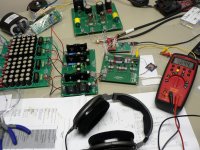
What can I say, sound is very good, I'm using this DAC with Beta22 headphone amp. Here few shots,
Thanks
What can I say, sound is very good, I'm using this DAC with Beta22 headphone amp. Here few shots,
Thanks
Attachments
 A Happy new year to everyone
Hi
Having spent the festive break reading through the thread a few times I would like to make the following observations / suggests / questions.
1. If I build the boards (psu / salas shunts / dac) as per the diagrams and BOM then I should have a working DAC.
2. If the I2S source does not have a buffer then I need the new high-speed buffer board (at the moment I am sucessfully running I2s from a QA-550 into Buffalo 32S and from a juli@ into Buffalo II - since neither of these dacs seems to have a buffered input I assume there should not be a problem with the TDA1541A board!!).
3. It would be better to remove the TL431s and associated circuitry; in this case it would seem to be better to chop the board removing the TL431 section and wiring the Salas shunts as close as possible to the TDA1541A - a possible future version of the boards could have 3 parts for the DAC board - input psu connections board / TL431 board / DAC board? The Salas shunt boards could also have the outputs aligned to the DAC board allowing for even shorted connections?
4. Having a v2.3 board I do not have to lift any feet on the 74HC02.
5. Worry about the appropriate IV stage later!
If the above is correct then I will order all the bits (excluding TL431 bits) as per Ryelands excellent spreadsheet and get building.
Regards
Alan
Pre Orders:
Malka07 - 1x - Dispatched
studiostevus - 1x - Dispatched
Crusty - 1x - Dispatched
kamaths - 1x - Dispatched
av-trouvaille - 1x - Dispatched
ernesternest - 1x - Dispatched
noizas - 2x - Dispatched
Ryelands - 3x - waiting for shipment on request
dsolodov - 1x - Dispatched
Malka07 - 1x - Dispatched
studiostevus - 1x - Dispatched
Crusty - 1x - Dispatched
kamaths - 1x - Dispatched
av-trouvaille - 1x - Dispatched
ernesternest - 1x - Dispatched
noizas - 2x - Dispatched
Ryelands - 3x - waiting for shipment on request
dsolodov - 1x - Dispatched
Hi Alon,
to your questions:
You still need an output stage.
Unfortunately i don´t know the two I2S devices.
As i wrote before, if your I2S devices supply voltages equals 3.3V and don´t have a buffer IC on board,
you would need one, e.g. my Ultra High Speed Buffer Module.
The I2S attenuators from ecdesigns i am using on my DAC module, are designed for 5V TTL levels only.
So we need the buffer between the output of these 3.3V devices and the input of my DAC module
for a proper work, without canceling the advantages of the I2S attenuators.
The main advantage of my DAC project is the modular design.
For those who could not or don´t want use the HighEnd Salas Shunt Modules,
the additional TL431 are still on the DAC module for best voltage regulation.
I think Lucas had connected the Salas Shunt´s directly to the DAC Module. If he is ready with his soundcheck, i hope he post his experiences.
A new revision with a separate TL431 board is not planned.
Correct.
Best regards,
Oliver
to your questions:
1. If I build the boards (psu / salas shunts / dac) as per the diagrams and BOM then I should have a working DAC.
You still need an output stage.
2. If the I2S source does not have a buffer then I need the new high-speed buffer board (at the moment I am sucessfully running I2s from a QA-550 into Buffalo 32S and from a juli@ into Buffalo II - since neither of these dacs seems to have a buffered input I assume there should not be a problem with the TDA1541A board!!).
Unfortunately i don´t know the two I2S devices.
As i wrote before, if your I2S devices supply voltages equals 3.3V and don´t have a buffer IC on board,
you would need one, e.g. my Ultra High Speed Buffer Module.
The I2S attenuators from ecdesigns i am using on my DAC module, are designed for 5V TTL levels only.
So we need the buffer between the output of these 3.3V devices and the input of my DAC module
for a proper work, without canceling the advantages of the I2S attenuators.
3. It would be better to remove the TL431s and associated circuitry; in this case it would seem to be better to chop the board removing the TL431 section and wiring the Salas shunts as close as possible to the TDA1541A - a possible future version of the boards could have 3 parts for the DAC board - input psu connections board / TL431 board / DAC board? The Salas shunt boards could also have the outputs aligned to the DAC board allowing for even shorted connections?
The main advantage of my DAC project is the modular design.
For those who could not or don´t want use the HighEnd Salas Shunt Modules,
the additional TL431 are still on the DAC module for best voltage regulation.
I think Lucas had connected the Salas Shunt´s directly to the DAC Module. If he is ready with his soundcheck, i hope he post his experiences.
A new revision with a separate TL431 board is not planned.
4. Having a v2.3 board I do not have to lift any feet on the 74HC02.
Correct.
Best regards,
Oliver
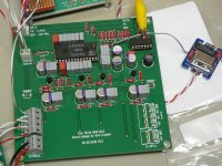
Hello Oliver
all ordered PCBs, including Ultra High Speed Buffer Modules, received.
Thank you very much.
Now will start with building.
Can you say that is best solution to solder those pcbs covered by gold with eutectic solder?
Almost all other producers of diy pcb, uses non gold immersion, because gold is ok for contacts, not for soldering.
Here is John Broskie opinion:
"If any of the parts have gold-plated leads, remove the gold flash before soldering the part, as only a few molecules of gold will poison a solder joint, making it brittle; use sandpaper, steel wool, or a solder pot.
NASA forbids any gold-contaminated solder joints; you should as well. (Yes, there are many quality parts with gold-flashed leads, but the use of gold is a marketing gimmick, not sound electrical engineering practice.)"
I use Cardas quad eutectic solder, but I have no solder pot for such big PCB. On other hand I can not use sandpaper or steel wool for removing gold from PCB.
Please advice
Saulius
Hello Oliver
all ordered PCBs, including Ultra High Speed Buffer Modules, received.
Thank you very much.
Now will start with building.
Can you say that is best solution to solder those pcbs covered by gold with eutectic solder?
Almost all other producers of diy pcb, uses non gold immersion, because gold is ok for contacts, not for soldering.
Here is John Broskie opinion:
"If any of the parts have gold-plated leads, remove the gold flash before soldering the part, as only a few molecules of gold will poison a solder joint, making it brittle; use sandpaper, steel wool, or a solder pot.
NASA forbids any gold-contaminated solder joints; you should as well. (Yes, there are many quality parts with gold-flashed leads, but the use of gold is a marketing gimmick, not sound electrical engineering practice.)"
I use Cardas quad eutectic solder, but I have no solder pot for such big PCB. On other hand I can not use sandpaper or steel wool for removing gold from PCB.
Please advice
Saulius
Hi Saulius,
first a happy new year to you
")
Don´t be afraid of any solder problems. You colud use any lead and lead free solder you want.
I for myself use normal leaded 60/40 solder and Mundorf MSolder silver/gold.
BTW, all my modules are designed to play not in orbit.
Hi Oliver,
happy new year to you too
thanks for fast answer.
I agree to your advice that those diy devices are not going to play anywhere in outer space.
But, if NASA devices suffer many G overloads for short period, then audio equipment suffers micro-G overloads for many years
So this is not "snake-oil" issue: we need to take into account that "cold joint" is quite "popular" in audio devices, especially in older than 10 -15 years.
Maybe I hope to use assembled devices tiil end of my days.
This is why eutectic solder is better.
Simply, please take into account for future orders on PCB - gold is not always welcome, better cover solderable contacts with Rosin alloy.
Saulius
happy new year to you too
thanks for fast answer.
I agree to your advice that those diy devices are not going to play anywhere in outer space
. But, if NASA devices suffer many G overloads for short period, then audio equipment suffers micro-G overloads for many years
So this is not "snake-oil" issue: we need to take into account that "cold joint" is quite "popular" in audio devices, especially in older than 10 -15 years.
Maybe I hope to use assembled devices tiil end of my days
.This is why eutectic solder is better.
Simply, please take into account for future orders on PCB - gold is not always welcome, better cover solderable contacts with Rosin alloy.
Saulius
. . . poll at the start of the thread.
What are the differences between the finishes?
(It's perhaps a bit like voting in an election - no-one knows what the differences are but it doesn't really matter because what you vote for will never be what you get
)What are the differences between the finishes?
There is a nice illustration on the webside from multipcb between the Surface Finishes.
The only one that they don´t produce is the OSP surface finish.
Hi Ryelands
difference between finishes is simple - solder should have same metal in alloy formula, because "foreign" metal dissloves in solder joint in case of overheating, producing intermetallic compounds, which make joint unstable for current, wet and vibration.
You can check wikipedia for more detailed info.
By the way, gold is one of worst contaminants of solder joint
Most of audio diyers use common solders, based on tin with alloying parts of silver and copper.
If you gonna use eutectic solder, only few of them have gold included and almost all of them are VERY expensive as part of gold is above 80 percent.
This is why I asked for Oliver's advice about soldering gold plated PCB.
IMO, finishes in priority should be: tin, silver, OSP. No way gold.
But if you already have gold plated PCB or component leads (like me now) , here is a good way too - use solder with a lot of tin - it helps a bit.
Saulius
difference between finishes is simple - solder should have same metal in alloy formula, because "foreign" metal dissloves in solder joint in case of overheating, producing intermetallic compounds, which make joint unstable for current, wet and vibration.
You can check wikipedia for more detailed info.
By the way, gold is one of worst contaminants of solder joint
Most of audio diyers use common solders, based on tin with alloying parts of silver and copper.
If you gonna use eutectic solder, only few of them have gold included and almost all of them are VERY expensive as part of gold is above 80 percent
.This is why I asked for Oliver's advice about soldering gold plated PCB.
IMO, finishes in priority should be: tin, silver, OSP. No way gold.
But if you already have gold plated PCB or component leads (like me now
) , here is a good way too - use solder with a lot of tin - it helps a bit.Saulius
Can you find out how thick gold layer is on your PCBs?
Hi Saulius,
the Immersion Gold thickness of my pcb´s is 1-3 microinch.
 Thanks Oliver
Oliver:
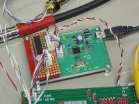
Thank you for the Ultra High Speed Buffer board. Mine has arrived today. What are P/N for fixed terminal connections?
You could use normal 2.54mm terminals or the
Wago 236-402 type.
- Status
- This old topic is closed. If you want to reopen this topic, contact a moderator using the "Report Post" button.
- Home
- Group Buys
- "Reference" TDA1541A DAC with I2S-BUS architecture