Yep, the 10k did the job right. My wife heard the amp and said everything is so crystal clear. I might get this one instead of buying an ALPS;
Dact Type 21 Stepped Attenuator Volume 10K FOR Preamp | eBay
I bought some in the past (100K) for some tube amps and they sound good.
BR,
Eric
Dact Type 21 Stepped Attenuator Volume 10K FOR Preamp | eBay
I bought some in the past (100K) for some tube amps and they sound good.
BR,
Eric
Last edited:
Well, still thrilled with this new amp. Very musical, I really enjoy it. Give it a try folks.
I have a quick question ; why do most amplifier have their VAS BJT or JFET tied together with a tie-wrap and some thermal paste...both BJT being at the same temp what does that do to the amp...is it to improve thermal stability or improve sound. I'm using some LatMOS so I think thermal stability is no issue because of their negative temp coefficient.
On my PCB, my 2 x BJT are a bit far but if I replace them and I leave the legs long enough I could manage to have them thermo coupled...the question remains...is it worthed ?
Thanks,
Eric
are you referring to VAS transistor or to the input pair of transistors (LTP in most amplifiers).why do most amplifier have their VAS BJT or JFET tied together
Are you referring to Q1 and Q2 in the circuit from post 187 (or post 8)? If so, then it makes no difference. Leaving them neatly soldered with short legs is probably better.On my PCB, my 2 x BJT are a bit far but if I replace them and I leave the legs long enough I could manage to have them thermo coupled...the question remains...is it worthed ?
Tying two input transistors together as you can describe can offer a tiny advantage in some circuits. By keeping them at the same temperature, it avoids any small changes in DC offset that would be caused by differences in temperature between the two transistors.
Reasons not to worry about it:
a) We're talking about a very small change, maybe a couple of millivolts, which is insignificant.
b) The normal DC offset is likely to be much higher than that.
c) DC offset is going to change slightly with changes in ambient temperature anyway.
d) The output of this circuit is AC coupled, so the DC offset doesn't appear at the speaker.
Last edited:
Q1 & Q2 are input transistors.
The current flowing in each determines the output currents.
If the currents in each are identical and all the other resistances are identical then the output offset will be zero.
If the current in one input transistor drifts slightly way from it's complement then the output offset drifts.
If you can Thermally Couple the two input transistors so that each drift by the same amount, then the output offset is virtually zero over a range of temperatures.
I’m a slow starter, was occupied by other stuffs, but I’m back with trying to build this power amp. I’ve already made a PCB for the power supply (yes, it’s a clone/simplified version of the DIYA Universal PSU, that PCB is out of stock so I downloaded KiCAD and draw/print some boards myself, as it’s for my personal use only I hope I’m not violating any rules).
I have some questions:
Thanks and regards.
- I’ll remove the jumper between the 2 halves of the PCB, to have 2 power supplies for the left and right channels respectively;
- Transformer with dual 18V secondary will be used, to power each of the 2 rectifiers and give 24V output;
- The resistors used are 0R47, so R is roughly 0R12 for the CRC filter;
- 8 x 22000uF 50V Panasonic capacitors are on their way to my home, to be installed into the board;
- Such a power supply maybe over-sized for this 7W amp, but my plan is to reuse it for some sort of F5 variant in the future
I have some questions:
- With a total of 17.6mF capacitance, do I need to worry about inrush current during power up, if so would a NTC (CL-60) be enough, or whether I should go for a full soft starter circuit;
- If I only install 4 of the caps (so 8.8mF total), would I avoid inrush current issue;
- What size of transformers to be purchased – would a 200VA 18V dual secondary be enough;
Thanks and regards.
Attachments
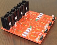
I’m a slow starter, was occupied by other stuffs, but I’m back with trying to build this power amp. I’ve already made a PCB for the power supply (yes, it’s a clone/simplified version of the DIYA Universal PSU, that PCB is out of stock so I downloaded KiCAD and draw/print some boards myself, as it’s for my personal use only I hope I’m not violating any rules).
- I’ll remove the jumper between the 2 halves of the PCB, to have 2 power supplies for the left and right channels respectively;
- Transformer with dual 18V secondary will be used, to power each of the 2 rectifiers and give 24V output;
- The resistors used are 0R47, so R is roughly 0R12 for the CRC filter;
- 8 x 22000uF 50V Panasonic capacitors are on their way to my home, to be installed into the board;
- Such a power supply maybe over-sized for this 7W amp, but my plan is to reuse it for some sort of F5 variant in the future
I have some questions:
- With a total of 17.6mF capacitance, do I need to worry about inrush current during power up, if so would a NTC (CL-60) be enough, or whether I should go for a full soft starter circuit;
- If I only install 4 of the caps (so 8.8mF total), would I avoid inrush current issue;
- What size of transformers to be purchased – would a 200VA 18V dual secondary be enough;
Thanks and regards.
I have some very BAD NEWS about Panasonic electrolytic capacitors.
http://www.mouser.com/PCN/Panasonic...aps_(ECO_s,_EET,_ECE_C,_ECE_T,_and_ECE_3).pdf
Member
Joined 2009
Paid Member
about Panasonic electrolytic capacitors.
"Due to declining market demand, Panasonic will discontinue
all Snap-In Aluminum Electrolytic capacitors."
whoa, when did snap-ins become obsolete ????
BTW
Nice amplifier design - and good to see no allergic reactions to use of an output cap
")
but does charge-up of cap make turn-on thump ? and turn-off thump ?
Last edited:
Yep, the 10k did the job right. My wife heard the amp and said everything is so crystal clear. I might get this one instead of buying an ALPS;
Dact Type 21 Stepped Attenuator Volume 10K FOR Preamp | eBay
I bought some in the past (100K) for some tube amps and they sound good.
BR,
Eric
Fair likely hood it's a cheap Clone.
Not really too much doubt at 12$ or am I just being suspicious?.. but that's irrelevant, IF it works reliably.. Does it?
Also does it have a ratchet/detent setup?
Inquiring minds
Q1 & Q2 are input transistors.
The current flowing in each determines the output currents.
If the currents in each are identical and all the other resistances are identical then the output offset will be zero.
If the current in one input transistor drifts slightly way from it's complement then the output offset drifts.
If you can Thermally Couple the two input transistors so that each drift by the same amount, then the output offset is virtually zero over a range of temperatures.
Thanks Andrew
Fair likely hood it's a cheap Clone.
Not really too much doubt at 12$ or am I just being suspicious?.. but that's irrelevant, IF it works reliably.. Does it?
Also does it have a ratchet/detent setup?
Inquiring minds
I had no idea it was a clone, a clone of what ? I've had them for a few months and so far so good.
I have never and will never spend big money on an attenuator, the best one is simply none...I normally use the remote volume control via JRiver (Gizmo on Android or JRemote for iPad.) I simply like the convenience of having a volume on each of the amp I build, having to carry a pre-amp gets on my nerves..LOL
BR,
Eric
Nice amplifier design - and good to see no allergic reactions to use of an output cap
but does charge-up of cap make turn-on thump ? and turn-off thump ?
It does sound good, I'm a huge fan of KISS theory.
I think the slow charging of C4 eliminates the turn-on thump but I do have a slight turn-off thump (very mild on my FE206E)
I had a big turn-on/off thump on my ACA, I had no choice but to add a switch at the output of the ACA. With this new amp, no such thing. I really enjoy both amp.
I do not have any allergic reaction to output cap.
BR,
Eric
Attachments
Last edited:
Hi Eric,
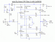
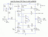
looking at the sch. (post #214) it seems to me that you misunderstood few things.
You wrote that the current through R6, R4 is 2.5mA but it's not. There is about 7mA flowing through R6, R4 (I=V/R=12.9 V / 1800 Ω)
Those 7mA branches on R9, R10 (about 4.5mA) and the rest (about 2.5mA) goes through Q1, Q2, R3, R5.
Hi Eric,
looking at the sch. (post #214) it seems to me that you misunderstood few things.
You wrote that the current through R6, R4 is 2.5mA but it's not. There is about 7mA flowing through R6, R4 (I=V/R=12.9 V / 1800 Ω)
Those 7mA branches on R9, R10 (about 4.5mA) and the rest (about 2.5mA) goes through Q1, Q2, R3, R5.
Thanks Juma,
You had mentioned the 2.5mA at the beginning and I never understood where that value came from, now I know
Is the attached schematic more realistic ?
Thanks,
Eric
Attachments
Hi Sam,e_fortier, do you want to give us any direct sonic comparisons in your setup, between the ACA and this 7Watt mini-F5?
To answer you I would need to do a A-B comparison which I haven,t done.
I will get back to you once the casing of this new amp is finish...I work slow.
BR,
Eric
... Is the attached schematic more realistic ?
Yes, that's more like it.
It's just that I'm still confused about high Vgs value for nominal Id (2.7V @ 0.7A). In the Cubie amp I get that much Id with Vgs of 1.6V. But then again, not all LATFETs are created equal...
- Home
- Amplifiers
- Pass Labs
- Recommendation for 5-10W amp.