Hi All,
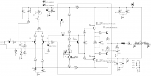
here is the layout I have come up with as a first pass. It follows exactly the layout by OS, but some modifications.
Changes:
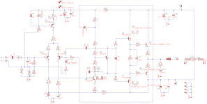
1. Zobel ground was not connected in original (latest) layout by OS.
2. C12 was missing from the layout
3. i/p filter cap drawn separately.
4. incorporated ground lifting diodes at i/p
5. C13 drawn separately for convenience (mine)
The top layer(purple) traces can be wires /jumpers for single side PCB. min trace clearance >24 mils.
The layout can be further optimized/ miniaturized a bit, but I thought comments from people, especially the designer, OS would help in saving some labor . Hope he hasn't unsubscribed from this thread and can post some comments.
Reg
Prasi
here is the layout I have come up with as a first pass. It follows exactly the layout by OS, but some modifications.
Changes:
1. Zobel ground was not connected in original (latest) layout by OS.
2. C12 was missing from the layout
3. i/p filter cap drawn separately.
4. incorporated ground lifting diodes at i/p
5. C13 drawn separately for convenience (mine)
The top layer(purple) traces can be wires /jumpers for single side PCB. min trace clearance >24 mils.
The layout can be further optimized/ miniaturized a bit, but I thought comments from people, especially the designer, OS would help in saving some labor
. Hope he hasn't unsubscribed from this thread and can post some comments.Reg
Prasi
Attachments
Believe it or not, its Eagle, a program most people hate on this forum. I tried switching to diptrace, but you know its become like, "you cant teach an old dog, new tricks".Dear Prasi,
Which is the program you are using fir the schematic and Pcb ? is it Diptrace ?
reg
prasi
Thanks prasi, I'd be much obliged if you could. I'd like to etch them on to 150mm x 150mm board that I already have. I don't mind generous spacing as I might be drawing it by hand !
ostrippers version looks easy to copy.
ostrippers version looks easy to copy.
ABSOLUTELY my intentions , not to compete with Carlos , or to steal, that is why I try to catch all mistakes - and pay close attention to details.
The FINAL version with no errors.. (almost sure):
An externally hosted image should be here but it was not working when we last tested it.
Last edited:
Dedicated to Ostripper!.
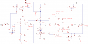
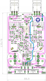
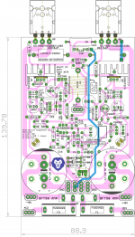
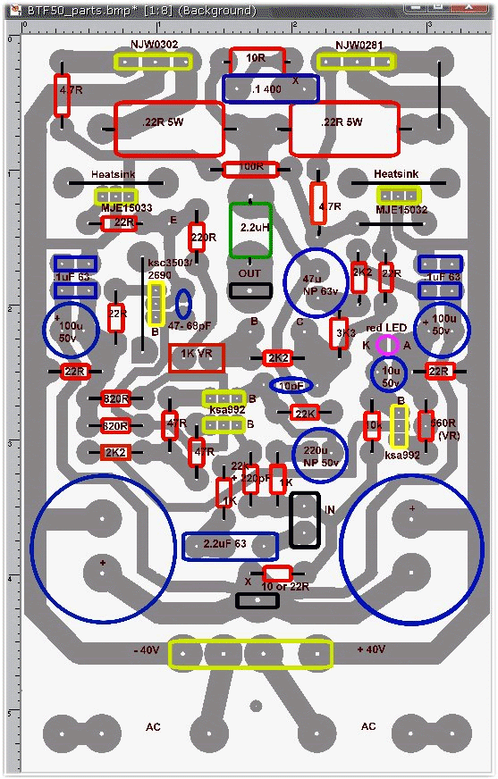
Here is what I could come up with quickly. Layout is totally based Ostripper's original layout, but slight modifications where I found convenient (to remove jumpers, etc).
reg
Prasi
Here is what I could come up with quickly. Layout is totally based Ostripper's original layout, but slight modifications where I found convenient (to remove jumpers, etc).
reg
Prasi
Attachments
Last edited:
Hi,
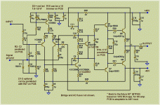
today I discovered this old thread and read it with great curiosity. Though I couldn't manage to get a copy of the 1972 RCA Transistor Manual, but I dowloaded the 1982 issue. The topic of this discussion basically is on a design shown at page 182 of this manual, isn't it?
Now would you please look at pages 191 and 196, respectively. Both circuit diagrams are on basically very similar designs with the main difference in the output section, one being true complementary and one being quasi complementary. But I wonder why RCA uses different opamps at the inputs, CA3140A in the true complementary and CA3100A in the quasi complementary design. As the input and the output sections in both designs are separated/connected by a almost identical level translator circuitry, involvong the first four transistors, it makes me wonder what's the purpose of using different opamps? What's the difference between CA3140A and CA3100A that makes one suitable for a true complementary and the othe one for a quasi complementary output stage? Any thoughts are welcome!
The reason for my question is that I've a bag of 2N4348's lying around here. This thread now makes me thinking of building a pair of real old school quasi complementary power amplifiers, or maybe a stereo one, featuring five power devices in parallel per side, driven by another one each. As the CA3100A has become unobtanium these days, and the CA3140A still is available and cheap, I'd like to substitute it by the latter one.
EDIT: As I've got a copy of the 1978 RCA datasheet/application note for the BD550 family of power devices, and the last application there, a 300 watts amplifier, features the same topology around the CA3100A, I suspect that this IC might be the predecessor of the CA3140A, appearing in the true complementary designs published four years later.
Hi Prasi,
I suspect both the circuitry and the PCB layout are lacking a junction from Q4's collector to Q5's emitter, don't they?
Best regards!
today I discovered this old thread and read it with great curiosity. Though I couldn't manage to get a copy of the 1972 RCA Transistor Manual, but I dowloaded the 1982 issue. The topic of this discussion basically is on a design shown at page 182 of this manual, isn't it?
Now would you please look at pages 191 and 196, respectively. Both circuit diagrams are on basically very similar designs with the main difference in the output section, one being true complementary and one being quasi complementary. But I wonder why RCA uses different opamps at the inputs, CA3140A in the true complementary and CA3100A in the quasi complementary design. As the input and the output sections in both designs are separated/connected by a almost identical level translator circuitry, involvong the first four transistors, it makes me wonder what's the purpose of using different opamps? What's the difference between CA3140A and CA3100A that makes one suitable for a true complementary and the othe one for a quasi complementary output stage? Any thoughts are welcome!
The reason for my question is that I've a bag of 2N4348's lying around here. This thread now makes me thinking of building a pair of real old school quasi complementary power amplifiers, or maybe a stereo one, featuring five power devices in parallel per side, driven by another one each. As the CA3100A has become unobtanium these days, and the CA3140A still is available and cheap, I'd like to substitute it by the latter one.
EDIT: As I've got a copy of the 1978 RCA datasheet/application note for the BD550 family of power devices, and the last application there, a 300 watts amplifier, features the same topology around the CA3100A, I suspect that this IC might be the predecessor of the CA3140A, appearing in the true complementary designs published four years later.
Dedicated to Ostripper!.
Here is what I could come up with quickly. Layout is totally based Ostripper's original layout, but slight modifications where I found convenient (to remove jumpers, etc).
reg
Prasi
Hi Prasi,
I suspect both the circuitry and the PCB layout are lacking a junction from Q4's collector to Q5's emitter, don't they?
Best regards!
Last edited:
Hi Kay, I can only say this, what eyes you got!!! amazing.... Here is the revised artwork.Hi,
today I discovered this old thread and read it with great curiosity. Though I couldn't manage to get a copy of the 1972 RCA Transistor Manual, but I dowloaded the 1982 issue. The topic of this discussion basically is on a design shown at page 182 of this manual, isn't it?
Now would you please look at pages 191 and 196, respectively. Both circuit diagrams are on basically very similar designs with the main difference in the output section, one being true complementary and one being quasi complementary. But I wonder why RCA uses different opamps at the inputs, CA3140A in the true complementary and CA3100A in the quasi complementary design. As the input and the output sections in both designs are separated/connected by a almost identical level translator circuitry, involvong the first four transistors, it makes me wonder what's the purpose of using different opamps? What's the difference between CA3140A and CA3100A that makes one suitable for a true complementary and the othe one for a quasi complementary output stage? Any thoughts are welcome!
The reason for my question is that I've a bag of 2N4348's lying around here. This thread now makes me thinking of building a pair of real old school quasi complementary power amplifiers, or maybe a stereo one, featuring five power devices in parallel per side, driven by another one each. As the CA3100A has become unobtanium these days, and the CA3140A still is available and cheap, I'd like to substitute it by the latter one.
EDIT: As I've got a copy of the 1978 RCA datasheet/application note for the BD550 family of power devices, and the last application there, a 300 watts amplifier, features the same topology around the CA3100A, I suspect that this IC might be the predecessor of the CA3140A, appearing in the true complementary designs published four years later.
Hi Prasi,
I suspect both the circuitry and the PCB layout are lacking a junction from Q4's collector to Q5's emitter, don't they?
Best regards!
I am not sure of the answer to your question on 2N4348, may be someone else can answer.
reg
Attachments
Hi Kay, I can only say this, what eyes you got!!! amazing.... Here is the revised artwork.
TAL
!I am not sure of the answer to your question on 2N4348, may be someone else can answer.
reg
My question primarily is on CA3100A vs. CA3140A, rather than on the 2N4348's. Perhaps it might be more suitable to ask it in the »Parts« section of this board?!?
Btw, would the 2SC5200/2SA1943 pair of output devices also be reasonable for the true complementary circuitry and the PCB you were showing to us?
Best regards!
TAL
My question primarily is on CA3100A vs. CA3140A, rather than on the 2N4348's. Perhaps it might be more suitable to ask it in the »Parts« section of this board?!?
Btw, would the 2SC5200/2SA1943 pair of output devices also be reasonable for the true complementary circuitry and the PCB you were showing to us?
Best regards!
Yes original 2sc5200/2sa1943 should work well.
Thanks prasi, I'd be much obliged if you could. I'd like to etch them on to 150mm x 150mm board that I already have. I don't mind generous spacing as I might be drawing it by hand !
I think I am done with my fine tuning. Still plan to build this? Then I can post pdf. do you find the posted design suitable for your requirements?
Yes original 2sc5200/2sa1943 should work well.
Thanks, Prasi, much appreciated!
But, as I've got some pairs of these lying around here, how to tell originals from counterfeits?
And, up to which rail voltages do you think a reliable operation is possible with just one pair of power devices?
I think I am done with my fine tuning. Still plan to build this? Then I can post pdf. do you find the posted design suitable for your requirements?
Yes, definitely (at least for mine
)! This design is missing the overload/short circuitry protection that has been with the RCA originals. Thus, an amplifier built according to your suggestion would solely work within an active loudspeaker enclosure, without any external connections (except the signal input and the mains power supply, of course).Best regards!
You could set up a DC load test for the 1943, or 5200.
Pass 2Adc through the transistor, by adjusting the base voltage. Use a 0r1 emitter resistor so you can check actual current Ie.
If you have a variable supply you can start with 5Vce for 10W dissipation and after a few minutes of stability, start increasing the Vce in 5V steps. Allow a few minutes after reaching constant current to see just how hot the heatsink and Tc become. Measure these.
You can use the SOA with temperature de-rating for Tc to see how close you can get to Toshiba's specification.
BTW,
I chose 2A rather than 1A to avoid going past the voltage knee into the second breakdown region. Don't use a big sink. Try 3C/W to 5C/W, it will get very hot.
I did this test for a BD139 and was surprised how long it operated at way above de-rated SOA. I seem to recall it was at >150% for more than a couple of hours.
Last edited:
Hi Kay, I can only say this, what eyes you got!!! amazing.... Here is the revised artwork.
I am not sure of the answer to your question on 2N4348, may be someone else can answer.
reg
Hi Prasi
R29 should return to main ground not signal ground.
Those drivers are very robust and suited to the task. The only time I have experienced cross-conduction was when using the speed up cap (C13). Personally I would get rid of it. You should be able to eliminate those output base stoppers if the layout is good. Provided the drivers are well heatsinked, you might increase the standing current further to 30mA (R19 = 47R).
Hi Kay,Thanks, Prasi, much appreciated!
But, as I've got some pairs of these lying around here, how to tell originals from counterfeits?
And, up to which rail voltages do you think a reliable operation is possible with just one pair of power devices?
Yes, definitely (at least for mine
Best regards!
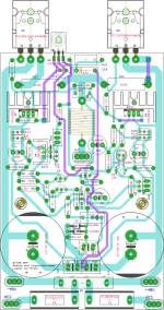
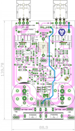
Posting herewith pdf for etching. All views from component side. Please tell me if you need anything different.
Also if you indeed build and test it, please share your impressions here.
Yes, there is no short circuit protect here. you could use a simple start delay / dc protect available on the diyaudiostore and a crowbar protect like APEX design posted by me here http://www.diyaudio.com/forums/solid-state/173462-studio-reference-amplifier-222.html#post4837066 . The beauty is you dont need separate supply for this crowbar protect and can be directly mounted on the speaker binding posts of the amplifier cabinet or speaker box.
It is very difficult to tell counterfeit from original. If the ones you got come from a reputed supplier like farnell/mouser, etc or removed from very old working amplifier, then they are originals.
Hi Prasi
R29 should return to main ground not signal ground.
Those drivers are very robust and suited to the task. The only time I have experienced cross-conduction was when using the speed up cap (C13). Personally I would get rid of it. You should be able to eliminate those output base stoppers if the layout is good. Provided the drivers are well heatsinked, you might increase the standing current further to 30mA (R19 = 47R).
Hi Christian,
Thank you for taking a look at this. I have incorporated your suggestions as options that one can try and see for himself.
Regarding return of R29, Ostripper had its return to the SGND in one the schematics i found on his website (attached). So I have kept the option of returning it to PGND as default or to SGND as option.
reg
prasi
Attachments
R29 should return to main ground not signal ground.[/quote
Agreed to that. But I'd return the input RCA's ground lugs to the main ground star also, so that wouldn't matter all too much.
Best regards!

Those drivers are very robust and suited to the task. The only time I have experienced cross-conduction was when using the speed up cap (C13). Personally I would get rid of it. You should be able to eliminate those output base stoppers if the layout is good. Provided the drivers are well heatsinked, you might increase the standing current further to 30mA (R19 = 47R).
Hi,
what about dividing R19 into two separate resistors about half the value each and referring their junction to the junction of R22 and R23?
Best regards!
- Status
- This old topic is closed. If you want to reopen this topic, contact a moderator using the "Report Post" button.
- Home
- Amplifiers
- Solid State
- RCA 1972 Basic amplifier MODS