lineup said:So the nightmare is to connect a power supply ripple filter electrolytic
to ground close to or in same rail as The Input of signal.
This is a very important and basic point, and I had taken care of this. I had separated out the signal ground point (INGND) from the power ground points (PGND1 and PGND2). Slone too emphasises this in his power-amp books.
But Self seems to go one step further and says that supply decoupling caps which are close to the output devices are likely to inject even more serious ripples and noise into the grounds, and their grounded ends should probably be separated even from the rest of the power grounds.
Yes, that's what I've already done in my three ground points by now, but reading Self, I almost got the impression that he is advocating a separate low-inductance path to the off-board star-ground point for just the output-stage decoupling caps. He almost seems to want to see separate wires from the grounded ends of those caps to the off-board ground, sort of like Mike Bettinger was saying.pinkmouse said:That's where on-board star grounding helps.
Hi,
re post60,
C1 can be deleted and then R1+R2 can be combined.
It will allow a little more power supply ripple through to the tail of the LTP.
It can be measured. But can you hear it?
Once you have move the Thiel network to the speaker terminals then the next biggest Power supply ground comes from the decoupling.
The grounds at the voltage amp end are nearly constant current and to help even more they are very small currents.
Okay, cool. And if the purpose of the cap is to absorb some ripple, then I guess I can use one cap to handle the decoupling of two CCS?AndrewT said:C1 can be deleted and then R1+R2 can be combined.
It will allow a little more power supply ripple through to the tail of the LTP.
It can be measured. But can you hear it?
tcpip said:
He almost seems to want to see separate wires from the grounded ends of those caps to the off-board ground, sort of like Mike Bettinger was saying.
My point was that I've found wires of almost any length to be ineffective in this application, hence the use of the chassis or no caps at all.
Regards, Mike.
tcpip said:
Okay, cool. And if the purpose of the cap is to absorb some ripple, then I guess I can use one cap to handle the decoupling of two CCS?
I think AndrewT advice of removing C1 in current source is alright.
The ultimate solution, used by perfectionists,
would be
Replace C1, R1, R2 with a JFET current source
I use many times JFET in, my BJT Bipolar amplifiers,
as current sources for my BC550C/BC560C LTP (long tailed pair) CCS.
I guess you know howto setup JFET for CCS.
1 JFET
1 Resistor
The important thing is: use some JFET that can take 42 Volt!!!
This avoids some other tricks to reduce voltage across JFET.
BF245 takes 30V, 2SK170 takes 40V
2SK117 takes 50V, 2SK373 takes 100V
You better check this - but I think I remember jfet voltage correct.
Of course there are other JFETs possible for such a current source.
Those that I personally do not know of.
Yet.
Regards
lineup
sixtek said:Lineup,
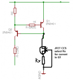
There is no need for min. 40-50V rated JFET if Tcpip chooses the following configuration (see attachment).
sixtek
I see what you mean.
This is an idea, of course. And it would work.
But using BJT, like 2N5401 for CCS to input pair might be better.
Besides 2N5401 takes more than 100 voltage,
JFET and BJT gives a bit different current, when used in current sources.
What I have understood, it has got something with capacitance in FET to do.
Maybe also noise is a factor.
-------------------------
So I still will recommend Tcpip
that he could, like I often do,
use one JFET CCS
to bias his 2N5401 current source.
Of course the final choice is his.
There are many ways to arrange a constant current source for
long tailed input pair stage.
Several of them would give equal good results.
Regards
lineup
I'll start by building it with no caps, then see.MikeBettinger said:My point was that I've found wires of almost any length to be ineffective in this application, hence the use of the chassis or no caps at all.
I was wondering about using the chassis... won't it cause the entire chassis to radiate EMI/RFI?
lineup said:The ultimate solution, used by perfectionists,
would be
Replace C1, R1, R2 with a JFET current source
Thanks guys, but I think I'll use the existing BJT-based CCS for this version of the amp, and try to see if the amp works at all. I'm starting with a tried and tested circuit, so I'm trying to make only very small changes. Most of my changes have been to do with PCB layout issues, component placement issues (on-board versus off-board), or changes to decoupling caps, etc.sixtek said:There is no need for min. 40-50V rated JFET if Tcpip chooses the following configuration (see attachment).
As you know, this is supposed to be a very well-known schematic, so I'm just trying to learn how to take a given schematic and translate into a real amp, making as littlle change to the schematic itself as possible.
Larger changes I'll make in the next round.
tcpip said:
Thanks guys,
but I think I'll use the existing BJT-based CCS for this version of the amp,
I have never suggested anything else!
You did not have time to read my post with my suggestion, did you?
Okay here I go again.
The ultimate solution, used by perfectionists,would be
Replace C1, R1, R2 with a JFET current source.
I use many times JFET in, my BJT Bipolar amplifiers,
as current sources for my BC550C/BC560C LTP (long tailed pair) CCS.
I guess you know howto setup JFET for CCS.
1 JFET
1 Resistor
So this is it:
Replace C1, R1, R2 with a JFET current source.
If you do this, you reduce disturbance from supply lines further.
= higher PSRR, most probably.
If you look at my attachment, you will understand.
And I can tell it is a good model, quite often used in good amplifiers.
The good thing, it will not complicate your amp very much.
You remove 3 components and add 2.
And get better, theoretically, current source for the input pair.
Regards
lineup
Attachments
You are half-right. I'd read your earlier post, but didn't understand it. I had thought (like the other poster) that you were suggesting that I should replace my BJT CCS with a JFET CCS. Now I have understood, after seeing your schematic.lineup said:I have never suggested anything else!
You did not have time to read my post with my suggestion, did you?
What does the FET do over and above the resistor in that ground leg? How does it work?
Can you give me the part number for the JFET? And will any small-signal FET do?
Thanks for the suggestion.
tcpip said:
I'll start by building it with no caps, then see.
Again, keep the power wires as short as reasonably possible.
Originally posted by tcpip I was wondering about using the chassis... won't it cause the entire chassis to radiate EMI/RFI?
Conceptually speaking there is a reason that antennas are normally constructed of wire, not of flat plates.
Regards, Mike.
tcpip said:
What does the FET do over and above the resistor in that ground leg?
How does it work?
Can you give me the part number for the JFET?
And will any small-signal FET do?

I answered 90% of those questions in my first post about this.
And if your friends in this project is just that: friends
They will inform you the rest.
There are many website links, we could learn 'bout using
JFET as Constant Current Source
As I did put it. See below:
I guess you know how to setup JFET for CCS.
1 JFET
1 Resistor
lineup said:
The ultimate solution, used by perfectionists,
would be
Replace C1, R1, R2 with a JFET current source
I guess you know how to setup JFET for CCS.
1 JFET
1 Resistor
The important thing is: use some JFET that can take 42 Volt!!!
This avoids some other tricks to reduce voltage across JFET.
BF245 takes 30V, 2SK170 takes 40V
2SK117 takes 50V, 2SK373 takes 100V
You better check this - but I think I remember jfet voltage correct.
Of course there are other JFETs possible for such a current source.
Those that I personally do not know of.
Yet.
.
Regards
lineup
A bit bothered about Nowadays people ability to READ ..
... and get one message correctly
... they know how to POST alright, plenty of posts
but how about reading, and understand the real main message
that somebody sender try to get through, to you

Attachments

I built an 11 .4 3 or 4 years back. Here are a few observations from actual experience building this.
A- Diode and resistor on the rails are not needed. Use Slone's advice about the capacitance/channel keep the wires from the PS twisted together as much as possible and away from the input wires and you will be fine.
B- 3x4 is a little crowded. Sloane uses a larger PCB which I think helps keep the output (high current) traces away from the input traces.
C- Keep L1 away from input and VAS. This may require a larger board. I like to take the Zobel network and L1 off the board and air-wire them at the inside of the binding posts. This will make the rest of the board easier to layout and seems reduce oscillation tendencies.
D- Since this is a CFB output it is true that optimum thermal tracking is done by mounting the Vbe transistor on of one of the drivers. One of Slone's books shows it and the two drivers mounted on the main heatsink along with the output devices which out to be the wrong way to do. However, I've tried it both ways and both woork just fine. That's kind of surprising but it works nonetheless <shrug>.
Continued.
With only a single set of output devices Oscillation isn't as fearsome as with parallel devices. I don't know why -- it just isn't. If oscillations occurr increasing the value of C9 may help. You have to experiment. Substituting MJ15003/4 for the output devices shown may also reduce oscilation tendencies. Both these expedients will increase THD but you can afford to sacrifice a little THD with this design. In any case, there is a good chance neither of these awill be neccessary.
If you have a scope you may see a little of what Self and Slone call "benign oscillation". It is distressing and unnerving to observe but, appearently it really is harmless. This amp would have been easier to build if I doidn't have a scope because then I would not have known about this and would not have spent so much time getting rid of it.
Final note: This is a very good sounding amp and woth the time and effort to build.
Thanks a lot for the inputs. Good to hear from you. I think you'd sent me the Vutrax files for this and the OptiMOS a couple of years ago. I managed to learn enough about Vutrax to be able to open and look at your PCB layout, and found Vutrax so frightening that I decided to try to build a new layout using Eagle.sam9 said:I built an 11 .4 3 or 4 years back. Here are a few observations from actual experience building this.
I'll keep your inputs in mind, and make changes to the design accordingly. I think just moving the LR and RC filters from the output to an off-board place will help clearing up the congestion somewhat.
What did you mean by "Slone's recommendations about capacitance/channel?" Did you mean his estimate of about 1000uF smoothing capacitance for every 10W of output power? In that case, I'll use 10,000uF per rail per Fig11.4 amp PCB that I build.
And by C9, you mean the second cap in the two-pole compensation scheme? Did you have to play around with its values? Should I be prepared for experimentation from the first round, and get myself a set of caps of different values and so on?
That's what i was referring to.lWhat did you mean by "Slone's recommendations about capacitance/channel?" Did you mean his estimate of about 1000uF smoothing capacitance for every 10W of output power? In that case, I'll use 10,000uF per rail per Fig11.4 amp PCB that I build.
That's the one. I hate to say get a bunch of caps in advance because if you don't need them it's wasted money. At the time I lived near an electronics surplus shop that had bins of silver-mica caps you could buy for 20-cents each. From the pictures, I think Slone uses ceramic . The procedure was to double the value and if the oscillation stops you are on the right track. Then reduce the value in the smallest steps available so long as the oscillation does not return. If this doesn't work, there is probably something wrong in the board layout. Even Self (who "knows everything") writes that CFB oscillations are difficult to diagnose.And by C9, you mean the second cap in the two-pole compensation scheme? Did you have to play around with its values? Should I be prepared for experimentation from the first round, and get myself a set of caps of different values and so on?
v8: with output L+R and R+C removed
Removed the output L+R and R+C circuits from the PCB, to make space for movement of components which will be needed for large heatsinks for VAS transistors.
Also removed the diodes from the supply lines... they are probably either unnecessary or a bad idea for this topology, as per feedback I've been studying.
An externally hosted image should be here but it was not working when we last tested it.
- Status
- This old topic is closed. If you want to reopen this topic, contact a moderator using the "Report Post" button.
- Home
- Amplifiers
- Solid State
- Randy Slone's "Fig 11.4" (Self's "Blameless"?): PCB layout