Hi tcpip
Part number-
I have not found a brilliant diode like the 1N4148 which works at higher voltages, but one I have used in such cases, is BAV21.
The CCS needs to be fast because, if it were slow, the output would not move quickly! Adding the base resistors multiplies the effect of the Miller capacitor (the VAS's own Cjc) which in the extreme would just stop the output rail moving...
Fully complementary was how Bailey described the EF output stage using NPN/NPN and PNP/PNP driver-outputs. I was referring to the driver/output pair. You can connect a small capacitor between the bases of the output pair when you use this arrangement to help shift charge. But a thought experiment shows that this could actually reduce the quiescent current by charging up after prolonged high frequency operation, something rather subtle and I have not had chance to properly assess this possible limitation. So use smallish capacitors (10-100nF so that the time constant isn't to high).
Yes 22 ohms will give you about 30 mA. The effect I described may not be quite this bad -there is an attenuation of the signal by the resistor after all - and at high frequencies beyond the -3dB point, the Miller effect cuts in to slow the stage down. So the critical point is around the -3dB point where the resistor loading has maximum effect, and it is this current which has to be available. Some say that transient distortion won't occur on normal signal levels because normal signals don't work this fast. I prefer to prevent any possible known problems. The point is that you may not need all 30 mA but I'd allow 25 mA at least.
I've found that the BD139-BD140 devices work very well as VAS and CCS stages up to 40V rails, may do a little more.
I don't recall the 649 is it a TO-92 version?
If so, for higher currents I recommend the TO-126 case. It would be about 800 mW for a 25 mA current at 35V and that'll need quite a sink to stay cool. With a Miller compensation I don't think you need to worry about lower Cob (Cjc) devices.
Cheers
John
Thanks. Got the datasheet from Digikey. Thirty-one cents. Good... now I know where to look when I need one.john_ellis said:I have not found a brilliant diode like the 1N4148 which works at higher voltages, but one I have used in such cases, is BAV21.
Okay. Will remember this.The CCS needs to be fast because, if it were slow, the output would not move quickly!
Okay. That's familiar (at least in name) then.Fully complementary was how Bailey described the EF output stage using NPN/NPN and PNP/PNP driver-outputs.
")
Yes, I too was talking about such values. Slone uses then now and then for EF outputs in his book.So use smallish capacitors (10-100nF so that the time constant isn't to high).
Okay. I'll keep this in mind when setting values for components. I'll do that 22Ohm I mentioned.The point is that you may not need all 30 mA but I'd allow 25 mA at least.
I was referring to 2SB649 and 2SD669 devices. Hitachi, I believe. They are either TO220 or TO126 (my datasheet says "TO126-mod"). Randy Slone and many others use these as driver transistors all over the place. The 2SB649 has Vceo > 120V, Ic of 1.5A, Vce(sat) of 1V, Hfe varying between 60 and 320 depending on version, Ft of 140MHz and power dissipation of 20W.I don't recall the 649 is it a TO-92 version?
How did you arrive at the 35V drop across the transistor? This is the sort of thing my shallow knowledge just doesn't permit me to understand.It would be about 800 mW for a 25 mA current at 35V and that'll need quite a sink to stay cool.
I've attached the 2SB649 datasheet.
Attachments
Hi tcpip
I only picked 35 V "out of the air" as this is typically what is needed for 50W into 8 ohms.
Obviously if you have more volts then the dissipation increases. The voltage to use is the one you have for one of your power rails. A better example might have been if you have 45V rails and set the VAS to 30 mA the dissipation will be 1.35W ....
Thanks for the data sheet. I like the 2SB649. Maybe I'll have to update my recommended VAS's now!
It'll have no problems running at 1.35W but you will need a good sink.
Cheers
John
Oh, I see. So I have to assume that this transistor will drop one full rail-to-ground voltage? Where does the rest go? Into the VAS transistor? (Sorry if I'm sounding dumb, but I'm really clueless about the inner workings of these things...)john_ellis said:I only picked 35 V "out of the air" as this is typically what is needed for 50W into 8 ohms.
Check out the feedback I got in this thread on my choice of VAS transistor. Apparently there are other much better devices. I believe the AKSA uses a different transistor, and the 2SB649/669 pair, being more than 5 years old, is now considered dated. I'm no expert; I'm just telling you what I've read.Maybe I'll have to update my recommended VAS's now...
Can you also check the idea of a separate CCS for the VAS? I've tried to put it in, into a very similar looking schematic from the other thread:
An externally hosted image should be here but it was not working when we last tested it.
Please look at Q18 and R41. Have I got it right? If yes, I'll make the change to this one's circuit too.
Hi tcpip
Well- a few things here to update too!
In this circuit you've got a 1 kohm load for the two-pole roll-off. This will need some pretty substantial current. The power supply voltage is 55V, so it seems to me that you'll need to allow 55 mA plus whatever the drivers need for the output stage.
Perhaps you don't need such a heavy load for another reason. In both your circuits, you've used 100 ohm emitter resistors on the input transistors.
I'm somewhat heretical on this point, but Miller stabilisation is not my favourite cup of tea. It can cause the input stages to overload, causing transient distortion at high frequencies, and one point of the input filter R33 C2 is to try to prevent this. THe argument is whether any real audio signals can ever be high enough to induce this slew-rate limit/transient intermodulation distortion or whatever you like to call it.
You can very easily prevent the input stage overloading, and avoid any debate about whether the amp. will or won't TIM. Giovanni Stochino showed that if you increase the current in the input stage, the input won't overload. All you have to do is to make sure that the voltage drop across the emitter resistors is large enough that neither transistor cuts off even for maximum input signals, but assuming that you get no feedback temporarily.
Stochino set the input stage currents to 10 mA, which gives 1V drop across 100 ohms, which should be enough for 2V peak input.
I think this is a little excessive, and a compromise I recommend is to use 330 ohm emitter resistors and 3 mA current each side, so your current source needs to be 6 mA. The down side is that the open loop gain drops, so your overall distortion is going to be higher.
BUt with 330 ohm emitter resistors, you don't need big capacitors in the Miller and you can make these smaller and the resistor load can be higher! So we're better all round now.
However, and there are always howevers, reducing the Miller capacitors may now mean that the highish Cjc (Cbo) of the VAS transistor might be more of a problem.
Let's see if we can set these right. I have not fully explored using FETS in the output stage, and I am suspicious that the configuration you have chosen might oscillate because you have complementary feedback pairs with gain. My recommendation is to use bipolars, or if you want FETS, to use "EF" type configuration and to avoid the gate voltage drive limit you'll need to raise the input stage rails to sit at 10-15 V higher than the output stage. Then you'll have a problem with setting the quiescent current I expect. So stick with bipolars and stick the drivers and outputs on one heatsink, bolt your bias stabliser to that and there you are.
If we pick 10 MHz as the unity gain point the total Miller capacitance needed for 330 ohm is only 47 pF! You might be able to do a two-pole job with a 470 pF in series and a 3.3k will give you extra gain up to 100kHz.
Now your VAS current need only be around 30mA to drive the twopole network at high frequencies.
I've nearly finished with the recommendations! Just a few minor points. I'm not convinced that you'll need the rectifier diodes in the power rails, these just drop volts and cause uneven loading currents. I'm not sure if feedback current pairs will oscillate or not. I prefer simple double diode, eg 2 1N4148 for biasing for the CCS, or a red LED. There was a thread on noise somewhere, but one advantage of the LED is that it gives you about 1.6V which balances the base voltage of the CCS better, as well as increasing the emitter resistor to give 1V drop instead of 600 mV to make a better CCS. With a red LED instead of your Q18, you'll need a 33 ohm resistor for R14.
For the input stage I invariably use a resistor-zener to give 10V and then another Zener at 5.6V on the base of the current source which decouples the power noise very effectively, and gives a solid constant current. (OK the zeners might be a little noisy). No capacitors!
You don't need a current source in the VAS stage - that will just stop the amp working. Instead, you can use this transistor as a protection device for Q6 but set the resistor R22 to about 10 ohms so that it limits at around double the normal current (60 mA in this case).
As I said, I'm not a fan of Miller amps, but if you're going to do one, I hope this is about the best you can do with it.
Sorry- thought of something else. If you're running at 55V you may need to change your 2SB649s as these are only 120V - I think you should try for a 150 or 160 V VAS/CCS pair. As the miller is now small I think you'll also need a low Cjc tranny!
Yes- you are right, the volts across the VAS/CCS pair is equal (very nearly) to the supply voltage when the output is sitting at zero.
Cheers
John
Not too many comments on the PCB layout in either thread on this amp.
Get the Zobel off the board and onto the output terminals.
Dump the output transistor bypass caps until you think you actually need them. Ground them separately to the heatsink, or anywhere to return them to whatever part of the supply you believe will absorb the energy; your current layout dumps it back into the input stage. Then try to figure out why they're needed, we're only amplifying audio frequencies here...
These two changes will give this thing half a chance of not being an oscillator.
The VAS transistors are going to need allot more heatsink at the current levels your running.
From the other thread I don't understand the diodes in the supply to the input stage. A simple resistor and a cap if you must. Don't place the supply to far away.
Suggestions only. Layout I do know, but I doubt I'll be trying to explain it. Just seen too many oscillators in my time.
Enjoy, Mike.
tcpip said:So the PCB has three points which will eventually connect to the off-board star-ground point. The two power grounds are PGND1 and PGND2, and the signal (and feedback) ground points go to INGND.
Flying visit!
You need to split up all your power and signal grounds and send them back to the main star separately. Where does INGND go? Just to the input sockets?
So you mean I should have something like half a dozen separate wires leading from various solder pads on the PCB to the star ground point?pinkmouse said:You need to split up all your power and signal grounds and send them back to the main star separately. Where does INGND go? Just to the input sockets?
I was thinking of connecting INGND straight to the input RCA, yes. I was not sure whether I should also drag a wire from the input RCA to the star ground. I was going to ask that question later on, after the PCB became a bit more stable.
The way I do it: Make two star grounds on your board, one for signal, one for power, then wire them back to the main star ground. Don't just use one track for the signal ground, as it can inject noise into sensitive sections, run each ground track back separately to one point. It's less critical for power grounds, but the more you can star the better.
Does this mean the PCB layout is adequate or has too many problems for you to discuss here?MikeBettinger said:Not too many comments on the PCB layout in either thread on this amp.
Okay. I can always keep them in the PCB, but not populate the components, I guess.Get the Zobel off the board and onto the output terminals.
I didn't understand "grounding them separately to the heatsink, or anywhere..." part. Do you suggest that if I put those caps at all, I should take separate ground wires from their other ends back to the star ground point?Dump the output transistor bypass caps until you think you actually need them. Ground them separately to the heatsink, or anywhere to return them to whatever part of the supply you believe will absorb the energy; your current layout dumps it back into the input stage.
Then try to figure out why they're needed, we're only amplifying audio frequencies here...
Yes, I figured that. I'll buy some large TO220 heatsinks and re-visit the PCB layout to make space for them, I think.The VAS transistors are going to need allot more heatsink at the current levels your running.
Those diodes are there in this schematic too. I was basically trying to protect the VAS and input stages during momentary supply voltage drops, during times when the OPS was sucking out a lot of current. During such brief periods, the input stage and VAS could receive current from C3+C14, C4+C15. That was the idea.From the other thread I don't understand the diodes in the supply to the input stage. A simple resistor and a cap if you must.
Okay.Don't place the supply to far away.
This is too tantalising. Do you expect that it's highly likely that this will be one of those oscillators, after I remove the OPS decoupling caps and move the output L+R, C+R circuits to the output socket?Layout I do know, but I doubt I'll be trying to explain it. Just seen too many oscillators in my time.
Got it.pinkmouse said:The way I do it: Make two star grounds on your board, one for signal, one for power, then wire them back to the main star ground.
The signal ground will just have two things coming and connecting to it, as far as I understand: one is the ground from the input circuit, and the other is the bottom of C7 (i.e. the feedback side). You mean I should run separate tracks for these two things to the INGND point? I think that should be doable. For the power grounds, I'll have to struggle more, but let me see what I can do.Don't just use one track for the signal ground, as it can inject noise into sensitive sections, run each ground track back separately to one point.
Have I understood you right?
I'm still studying your reply, and I'll take a bit of time to understand most of your suggestions properly. Specially, the impact of increasing that resistor in the middle of the two-pole compensation circuit will take a bit of time to sink in. There's only one point I wanted to point out, however....john_ellis said:Well- a few things here to update too!
Here, I just wanted to point out that this thread is about a BJT CF OPS circuit, not the FET circuit. That's in the other thread. Both circuits look very similar, but I am trying to learn from both separately. I won't make this circuit into a FET circuit... it'll be a BJT CF OPS, and I'll try to see what I need to do to get it to work well.Let's see if we can set these right. I have not fully explored using FETS in the output stage...
I have posted the L-MOSFET schematic here yesterday just to ask for your feedback for the VAS CCS. I wanted to know whether I've done it right. This circuit will remain a BJT CF OPS, it won't become an L-MOSFET circuit.
I'm really sorry if I'm confusing you (or others).Okay. I'd heard that one amp had used this D+R+C combo to get cleaner sound, so I was thinking of using it. I can always replace the D with a wire bridge when I build the amp, I guess.I've nearly finished with the recommendations! Just a few minor points. I'm not convinced that you'll need the rectifier diodes in the power rails, these just drop volts and cause uneven loading currents.
This part I think I understood. Is there any reason to prefer a red LED of 1.6V over a green one (1.85V, IIRC)? I understood why the R14 will need to be higher... it's going to drop a larger voltage.I'm not sure if feedback current pairs will oscillate or not. I prefer simple double diode, eg 2 1N4148 for biasing for the CCS, or a red LED. There was a thread on noise somewhere, but one advantage of the LED is that it gives you about 1.6V which balances the base voltage of the CCS better, as well as increasing the emitter resistor to give 1V drop instead of 600 mV to make a better CCS. With a red LED instead of your Q18, you'll need a 33 ohm resistor for R14.
This part I didn't understand. I think I'll have to look at a schematic somewhere which does this, to understand what you've described. Can you point me to something?For the input stage I invariably use a resistor-zener to give 10V and then another Zener at 5.6V on the base of the current source which decouples the power noise very effectively, and gives a solid constant current. (OK the zeners might be a little noisy). No capacitors!
I didn't understand this. You mean you recommend that there should be no CCS loading for the VAS?You don't need a current source in the VAS stage - that will just stop the amp working.
Yes, I understand that if I set R14 to allow 30mA VAS CCS current, then I'll need perhaps 10 Ohms for R22.... set the resistor R22 to about 10 ohms so that it limits at around double the normal current (60 mA in this case).
Can you please point me to where I can read about non-Miller amps, with some explanations of how they work? Basically, like Self and Slone have explained Miller compensated amps, are there other books/articles which explain for a beginner how the non-Miller amps work?As I said, I'm not a fan of Miller amps, but if you're going to do one, I hope this is about the best you can do with it.
What alternate devices do you think I could use?Sorry- thought of something else. If you're running at 55V you may need to change your 2SB649s as these are only 120V - I think you should try for a 150 or 160 V VAS/CCS pair. As the miller is now small I think you'll also need a low Cjc tranny!
Thanks for the inputs.
So, if I take one track from the bottom of C7+D1 to INGND, and another from the bottom of R4+C2 straight to INGND, then will I get it right? In that case INGND will be a star-ground for the signal, right?pinkmouse said:I see three tracks, INGND, and the bases of R4 and C7.
Hi,
I'm using 649/669 as drivers on +-58Vdc supply rails (Leach clone) and planned on +-42Vdc/+-52Vdc (Krell clones).
They have a good SOA for these voltages. 300mA @ 50Vce and 200mA @ 60Vce (12W @ 60Vce). There appear to be few devices that can better that at the speed & gain of these.
But if you are persuaded by reliability look at 649A/669A, 968, 1011, 1225, 1249, 1507, 1535, 1606, 1837, 1859, 1930,
compare SOA, gain, speed, Cob in that order. All of these claim higher Vce0 but many have poorer SOA. I believe it's drive ability into reactive loading that matters. High gain in the output stage lessens the stress on the driver.
If you can live with slow, low gain, but want almost unburstable then MJE15034/5 are tremendous, particularly for PA work.
I didn't understand the question. Of course there will be one wire from the INGND solder-pad to the off-board main star.pinkmouse said:What about the connection to the off board main star?
Or are you saying I need two separate wires to the main star, one for the bottom of C2+R4, and one for the bottom of C7+D1? I'm confused again.
tcpip said:Does this mean the PCB layout is adequate or has too many problems for you to discuss here?
Okay. I can always keep them in the PCB, but not populate the components, I guess.
I didn't understand "grounding them separately to the heatsink, or anywhere..." part. Do you suggest that if I put those caps at all, I should take separate ground wires from their other ends back to the star ground point?
This is too tantalising. Do you expect that it's highly likely that this will be one of those oscillators, after I remove the OPS decoupling caps and move the output L+R, C+R circuits to the output socket?
I’m not trying to tantalize. I'm just looking at your layout and know from the experience that mixing anything that going on in the output stage with the input stage, which is exactly what you're doing with your power grounds, will get you chasing your tail for a long time. It's more fun to have the amp come up with half a chance of working first time.
There are a lot of examples of amps that place the zobels and bypassing conveniently on the amp PCB, and probably just about as many types of compensation and snake oil to make it look OK.
The bypass caps (if needed) need a Low-Z path around the circuitry back to the supply ground. I suggested the chassis as an easy after the fact tweak that normally satisfies this if the need arises. A solder tag tapped and screwed into the grounded heatsink, next to where the supply connects to the PCB (or better yet, next to the transistor leads) allows short leads on the caps.
My comment on not needing the bypass caps is based on my approach of building a design without the bandaides and adding them only if there is no other way to get it to the listening part.
Mike.
Hi tcpip
Sorry if there was a lot to read through ... I'll see if I can help with the bits you did not follow.
Increasing the twopole resistor is possible if the capacitors are made smaller, as this just keeps the time constants constant. Reducing the capacitors are possible if the input resistors are increased to keep these time constants tracking. Actually I think a better combination would be something like the twopole cap being 2 or 3 times the nominal Miller cap. not 10x, but then you do get bigger spikes as I mentioned before.
You can use a CF OPS, but there are only about two advantages over the EF: quiescent current stability and greater efficiency because the "saturation" voltage when one of the pair is on is lower than that of the EF pair. You won'tbenefit from this efficiency increase if you drop the voltage to the input stages, though!
Whether this gives best audio performance I think is perhaps an interesting point.
I'll try to undo the confusion over the CCS/VAS: of course, the CCS and VAS work together, but in your circuit,you had a transistor which looked as though it was trying to define a constant current in your VAS stage. The CCS is fine and uses the resistor values already discussed. The only use of the extra transistor looking at the VAS emitter resistor would be to prevent the VAS overloading. Otherwise, it just sets the VAS to a CCS = no signal.
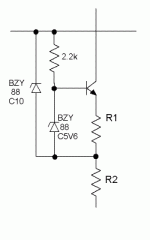
I think that the filter resistors on the power rails to the input stage are intended to stop power pulses reaching the input stages. The resistor is really the only effective component. As discussed in other threads, you may be better to use a separate supply voltage slightly higher than the output. But to keep you on track for a simpler circuit, try missing out the diode as you say. The current source I recommend works well at filtering noise from the rail it connects to for the input stage. I've attached the input current source for you. Originator of this was Bailey. (NPN version).
Not really, but the objective is to match the change of Vbe with temperature. I found that the old TI TIL209 gave an almost exactly constant current when the CCS transistor and diode were at room temperature and when they were dropped into boiling water (in a waterproof container). The change in diode voltage with temperature depends on the diode, so you may want to try a few devices. Almost any LED is probably going to be better than two silicon diodes (which always end up with over compensation).
AndrewT has said he uses 649's at 58V so maybe they're fine, you could also use 649A's; and I've used 968's.
The non-Miller approach is to wire the feedback capacitor from the VAS collector to the feedback transistor base. Nelson Pass seems to prefer this; Bailey used it (his amplifier is in a recent thread) and JLH used it. But maybe its not a beginners approach. It may need additional tweaks to roll the gain off to stop oscillations. Perhaps the JLH "70W" amp circuit might be a starting point. (HiFi News around the 1970's) Unfortunately my old copy of this was done before the latest generation of toner copiers - and has faded. Perhaps someone may help with this? I think with the increased VAS /CCS currents and anti-TIM input mods I've mentioned, the twopole Miller might be workable, and it should not TIM.
Cheers
John
Sorry if there was a lot to read through ... I'll see if I can help with the bits you did not follow.
Increasing the twopole resistor is possible if the capacitors are made smaller, as this just keeps the time constants constant. Reducing the capacitors are possible if the input resistors are increased to keep these time constants tracking. Actually I think a better combination would be something like the twopole cap being 2 or 3 times the nominal Miller cap. not 10x, but then you do get bigger spikes as I mentioned before.
You can use a CF OPS, but there are only about two advantages over the EF: quiescent current stability and greater efficiency because the "saturation" voltage when one of the pair is on is lower than that of the EF pair. You won'tbenefit from this efficiency increase if you drop the voltage to the input stages, though!
Whether this gives best audio performance I think is perhaps an interesting point.
I'll try to undo the confusion over the CCS/VAS: of course, the CCS and VAS work together, but in your circuit,you had a transistor which looked as though it was trying to define a constant current in your VAS stage. The CCS is fine and uses the resistor values already discussed. The only use of the extra transistor looking at the VAS emitter resistor would be to prevent the VAS overloading. Otherwise, it just sets the VAS to a CCS = no signal.
I think that the filter resistors on the power rails to the input stage are intended to stop power pulses reaching the input stages. The resistor is really the only effective component. As discussed in other threads, you may be better to use a separate supply voltage slightly higher than the output. But to keep you on track for a simpler circuit, try missing out the diode as you say. The current source I recommend works well at filtering noise from the rail it connects to for the input stage. I've attached the input current source for you. Originator of this was Bailey. (NPN version).
Is there any reason to prefer a red LED of 1.6V over a green one (1.85V, IIRC)? I understood why the R14 will need to be higher... it's going to drop a larger voltage.
Not really, but the objective is to match the change of Vbe with temperature. I found that the old TI TIL209 gave an almost exactly constant current when the CCS transistor and diode were at room temperature and when they were dropped into boiling water (in a waterproof container). The change in diode voltage with temperature depends on the diode, so you may want to try a few devices. Almost any LED is probably going to be better than two silicon diodes (which always end up with over compensation).
AndrewT has said he uses 649's at 58V so maybe they're fine, you could also use 649A's; and I've used 968's.
The non-Miller approach is to wire the feedback capacitor from the VAS collector to the feedback transistor base. Nelson Pass seems to prefer this; Bailey used it (his amplifier is in a recent thread) and JLH used it. But maybe its not a beginners approach. It may need additional tweaks to roll the gain off to stop oscillations. Perhaps the JLH "70W" amp circuit might be a starting point. (HiFi News around the 1970's) Unfortunately my old copy of this was done before the latest generation of toner copiers - and has faded. Perhaps someone may help with this? I think with the increased VAS /CCS currents and anti-TIM input mods I've mentioned, the twopole Miller might be workable, and it should not TIM.
Cheers
John
Attachments
- Status
- This old topic is closed. If you want to reopen this topic, contact a moderator using the "Report Post" button.
- Home
- Amplifiers
- Solid State
- Randy Slone's "Fig 11.4" (Self's "Blameless"?): PCB layout