You have not. As drawn each secondary winding now has a ground reference so you will end up with equal and opposite dc voltages. The supply impedance is very low (especially in a simulation) so the ground reference circuit (T15/16 on the original) will not work. If you look into the simulation carefully you will see Q1 turned hard on, desperately trying to 'lift' the floating ground reference and Q2 turned completely OFF. Compare this to the currents flowing in the schematic above it.Not so sure i've done things right with this one though, but the rails come out equal.
I haven't a clue either why they don't use a fully complementary output stage, but why do you think current dumping is a marketing idea? It has some rather obvious technical advantages, particularly that you can get low distortion out of an amplifier that doesn't have the usual thermal stability and transient crossover distortion problems.
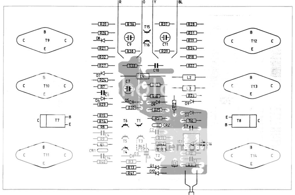
By the way, shouldn't T2 in the schematic of the first post be an NPN?
Yes, good catch I agree T2 should be NPN, looks like a cascode for the first gain stage of course.
I'm just saying that I don't see anything that looks like some sort of unique "current dumper", rather I see a fairly normal class B output stage. It is the bridge network that provides the distortion reduction. I'm not saying that it doesn't work, simply that the terminology is rather odd.
I'm just saying that I don't see anything that looks like some sort of unique "current dumper", rather I see a fairly normal class B output stage. It is the bridge network that provides the distortion reduction. I'm not saying that it doesn't work, simply that the terminology is rather odd.
Current dumping was a brand that Peter Walker used to market the amplifier. "Class C amplifier with feedforward error correction" doesn't quite have the same ring to it.
Regarding the quasi-complementary output stage:
- The QuAD 405 was released in 1975 when there were not a lot of good options for complementary output transistors
- As designed, the measured performance was exemplary for its day and not so shabby even now, even when the bridge components are non-selected parts.
- The bill of materials complexity and cost would have been lower.
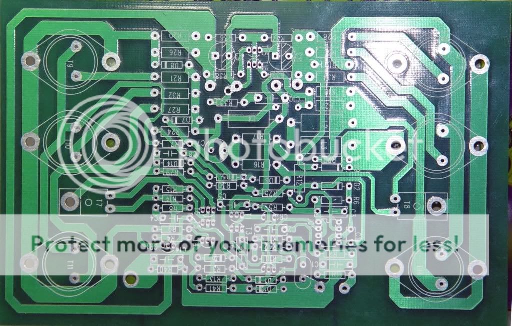
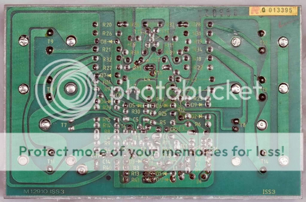
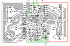
I found 2 errors in the pcb drawing which i've now fixed. (CR1 legs joined together and T2 legs joined together)
I've been looking at copper clad boards for making the pcbs. I've found a 203x114mm glass epoxy board with 35μm copper thickness. (1oz/ft) Will the copper be thick enough?
I've been looking at copper clad boards for making the pcbs. I've found a 203x114mm glass epoxy board with 35μm copper thickness. (1oz/ft) Will the copper be thick enough?
that depends on the length and width of the PCB trace and how much current you have...Will the copper be thick enough?
There are on-line calculators for determining the recommended PCB trace length/width for any current. It is worthwhile using these for the few high current traces on the board.
But in general 35um copper should be adequate for this design - unless you do soemthing really dumb like feeding the power rails through 0.2mm traces...
Traces are identical give or take 0.5mm or so to the original quad design. I have no idea how thick the copper on the original quad pcb is. Would help if i knew current levels for specific tracks at full power.
I've attached the up to date version of the pcb and layout.
I've attached the up to date version of the pcb and layout.
Attachments
Last edited:

Been looking through the components that i already have to see if i can use any in this project and came across some vishay MKP1837 47nF 160V caps. C10 in the schematic (+ output to ground) is rated at 250V. Would the rating of 160V be sufficient or should I just buy higher rated caps. (not exactly expensive, but its nice to use up stuff that I've got lying around)
I also noticed that I'd missed a hole out for the one connection on R12. (vertical resistor in between the line of 3 diodes)
I also noticed that I'd missed a hole out for the one connection on R12. (vertical resistor in between the line of 3 diodes)
Been looking through the components that i already have to see if i can use any in this project and came across some vishay MKP1837 47nF 160V caps. C10 in the schematic (+ output to ground) is rated at 250V. Would the rating of 160V be sufficient or should I just buy higher rated caps
160V rating is fine. This part will only see a sustained voltage equal to either supply rail. So a 63V rated part would be just OK, and a 100V part would give an excellent derating margin.
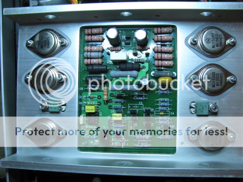
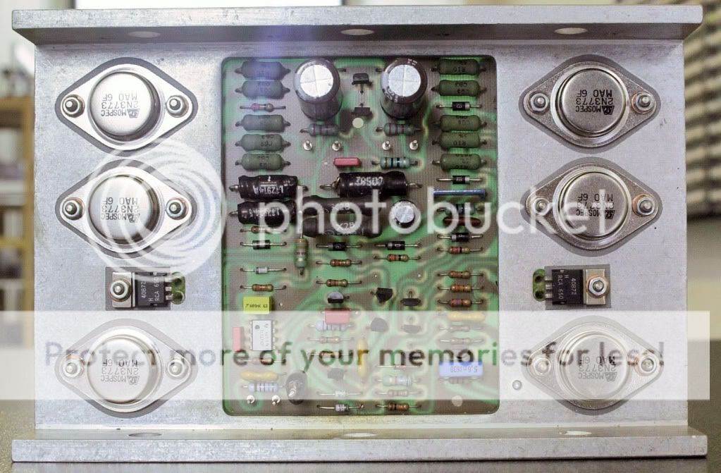
Yes the PCB design is derived from an image of an original pcb. It is an exact replica drawn 1:1 scale. I've test fitted 6 TO-3 devices just to make sure the holes were lined up properly. The original circuit overlaid on my tracing. I've also got a 707 pcb which looks like a computer designed version as the traces are all straight lines and constant widths.
Cad software that I have is Eagle 6.1 full, express sch/pcb and livewire/pcb wizard.
Cad software that I have is Eagle 6.1 full, express sch/pcb and livewire/pcb wizard.
Last edited:
I've got the ground plane layer on file as well it seems.
I am a tad confused as to why they did it as the original M12910 1 and 2 boards don't appear to have the ground plane layer yet the pcb layout is no different. (i've overlaid the issue 3 pcb onto the issue 1/2 pcb. The only difference i've found is the track positions in the bottom right corner. The connections are the same though.)

I am a tad confused as to why they did it as the original M12910 1 and 2 boards don't appear to have the ground plane layer yet the pcb layout is no different. (i've overlaid the issue 3 pcb onto the issue 1/2 pcb. The only difference i've found is the track positions in the bottom right corner. The connections are the same though.)
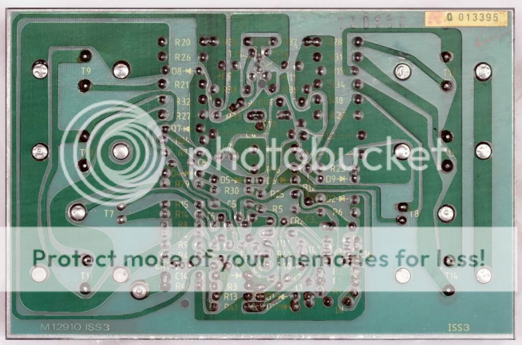
Spent the past 2 days reading up on this ground plane and its purpose. It seems it was introduced on issue 3 pcb's to help reduce interference from other appliances.
Here's what the service manual states for modifications:
(9) June '87 (SN 4500 approx) Shorting link of 16 SWG (1.5mm) tinned copper wire connected across PCB track earths. (see page 13) 330nF (C330NXA) capacitor C20 fitted across mains transformer primary. To reduce interference from electrical appliances (thermostats etc.)
(10) November '87 (SN 5700 approx) PCB iss. 3 introduced to improve screening and reduce interference from electrical appliances. R14, R15 and CR1 taken to R20 and R26 supply rail to improve performance.
Page 13: Fitting link to Issue 1 & 2 PCB
Mod 9 In cases of interference from household appliances, thermostats etc, connect a link across the track side of each amplifier printed circuit board as shown below.
(a) Scratch the protective lacquer from each PCB at the two points marked 'O' adjacent to 'C9, R3' and 'IN' respectively, and connect an insulated piece of 16 swg (1.5mm) tinned copper wire between these points as indicated.
(b) For very severe cases a 330nF 250V AC working capacitor (C20) may also be connected directly across the mains transformer primary connections.
These modifications were incorporated in production models with issue 2 PCB, from S/No 4500.
Wouldn't it be possible to just add a track like the attachment or is that poor design. If the track is not a good solution, is the quad wire mod any better?
Attachments
While i await an answer to the above point, I have some other things to consider.
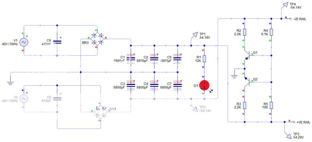
To improve upon the original design i am considering building a soft start circuit. The PSU design for my version uses a pair of 500VA transformers with 6x 6800uF capacitors per amp (12x in total) Not sure what would be best in this case? (whatever it is it'll need to be on a separate board to avoid the need to modify the amp PCB. I'd also prefer it to not require its own separate power supply/transformer. Been reading ESP pages here.) Biggest question is will it require a soft start circuit?
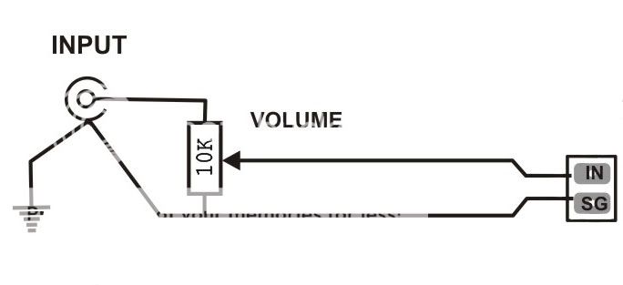
I also want to incorporate a gain control as the preamp outputs from most units is higher than the 500mV this amp requires for full power out. Wiring in a mono pot in like so... (10K substituted for an appropriate value)
To improve upon the original design i am considering building a soft start circuit. The PSU design for my version uses a pair of 500VA transformers with 6x 6800uF capacitors per amp (12x in total) Not sure what would be best in this case? (whatever it is it'll need to be on a separate board to avoid the need to modify the amp PCB. I'd also prefer it to not require its own separate power supply/transformer. Been reading ESP pages here.) Biggest question is will it require a soft start circuit?
I also want to incorporate a gain control as the preamp outputs from most units is higher than the 500mV this amp requires for full power out. Wiring in a mono pot in like so... (10K substituted for an appropriate value)
Last edited:
- Home
- Amplifiers
- Solid State
- Quad 909 Clone