Shunty
I reheated all the soldering and the + rail that was wobbly seems to have settled. It does wobble a bit when you touch the screw on the 3296 potentiometer, but I assume that is normal (not sure which brand I used).
Pumpkin
I tested the voltage of the leds I used, and they were all within 1.8-2V, so did not replace them.
The voltage between the output caps is nicely 0, but voltage between GND and one cap remains a about 20V after the 25point turn pot clicks.
Given that there are output caps and I started this preamp long ago, I decided to try playing music anyway, just to see if it at least made music.
I connected it to an old squeezebox and Aleph J, and the hum was quite bad (volume at minimum, source not playing). Hum increases as volume is increased (source still not playing).
We then tried some music and it sounds very promising! If only I can get rid of the hum.
A few notes:
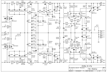
My pumpkin is set up for high gain (for F4). I changed R5/R6 to 150k (from 100k) and decreased C1/C2 to 3.3pF (from 5pF),
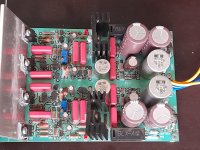
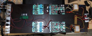
All parts are screwed to a long piece (>1m) of formply (plywood with coating, used in concrete industry) for testing, so not installed in a case. From left to right:
Two questions
1. How can I make sure my shunties are behaving themselves and not the cause of the hum?
2. What can be the reason I cannot get the voltage anywhere near zero between GND and any one of the output caps?
I reheated all the soldering and the + rail that was wobbly seems to have settled. It does wobble a bit when you touch the screw on the 3296 potentiometer, but I assume that is normal (not sure which brand I used).
Pumpkin
I tested the voltage of the leds I used, and they were all within 1.8-2V, so did not replace them.
The voltage between the output caps is nicely 0, but voltage between GND and one cap remains a about 20V after the 25point turn pot clicks.
Given that there are output caps and I started this preamp long ago, I decided to try playing music anyway, just to see if it at least made music.
I connected it to an old squeezebox and Aleph J, and the hum was quite bad (volume at minimum, source not playing). Hum increases as volume is increased (source still not playing).
We then tried some music and it sounds very promising! If only I can get rid of the hum.
A few notes:
My pumpkin is set up for high gain (for F4). I changed R5/R6 to 150k (from 100k) and decreased C1/C2 to 3.3pF (from 5pF),
All parts are screwed to a long piece (>1m) of formply (plywood with coating, used in concrete industry) for testing, so not installed in a case. From left to right:
- Aluminium bracket with mains input socket and fuse
- terminal block connecting mains to transformer primaries (secondaries soldered to the shunty boards)
- 2 x r-core transformer (each rated 2 x 45V 0.5A)
- 2 x shunties
- 2 x pumpkins
- 2 x 25k (cheap) stereo volume pots
- aluminium bracket with cinch and xlr inputs and outputs
Two questions
1. How can I make sure my shunties are behaving themselves and not the cause of the hum?
2. What can be the reason I cannot get the voltage anywhere near zero between GND and any one of the output caps?
1. How can I make sure my shunties are behaving themselves and not the cause of the hum?
2. What can be the reason I cannot get the voltage anywhere near zero between GND and any one of the output caps?
1. for start, just ground both inputs ( pos and neg) ditto at Pumpkin, then try settings; hardly that Shunty is culprit for hum, if you got proper voltages ...... and hardly that two Shuntys are reason for hum in two channels
2.increase R22 to 82R-100R, try again; or replace WR2 with 100R trimpot
I replaced R22 on both boards: from 47R to 100R. I am now able to get the voltage between TP0 and TP1 to zero, but not for long. There is a lot of drift, perhaps due to pcbs being screwed on a board, and testing in a possibly windy shed (so not a closed box).
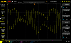
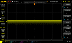
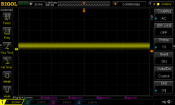
Anyway, I thought I would have a look at the Shunties first. It is years since I used my Rigol DS1054Z (I don't have much experience in using it) but I wanted to try it anyway. Note, no load.
These are the waveforms I got:
Shunty B NEG (CH4) and POS (CH3).
I have no reference, so have no idea if these waveforms are expected for the Shunty. I interpret is about 10mV p-to-p at a very high (MHz) frequency. I noticed my wheelchair produces a lot of RF noise, so did not move the wheelchair while making these measurements.
To me, the NEG waveform looks better than the POS, but this may be an artefact due to the color.
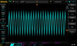
Shunty A NEG (CH2)
This waveform is similar to Shunty B NEG.
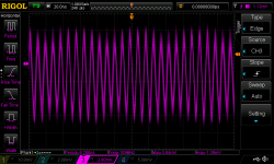
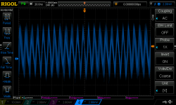
Shunty A POS (CH1)
I had trouble triggering on this one, as the voltage fluctuated and I could not get a screenshot at a low mV division. It had calmed down for a moment when I made the 50mV screenshot, but I was able to capture the wider spread later, at 200mV. I have attached 2 screenshots that show how wide the noise is. I also include a single shot.
I am out of my depth!
Question 1
Are the waveforms above normal for the Shunty?
Question 2
I have a lab power supply, but it has 30V max output. Can I test the pumpkins using the lab power supply at 30V (i.e. eliminating possible issues with the Shunties) to see if I can get 0V between TP0/TP1 and TP1/TP2?
My helper won't be back for 8 weeks (long holiday), and I don't know if I can find someone else to help me in the meantime. I would like a list of measurements to make to help diagnose this because he/she will probably not come again for a week.
Anyway, I thought I would have a look at the Shunties first. It is years since I used my Rigol DS1054Z (I don't have much experience in using it) but I wanted to try it anyway. Note, no load.
These are the waveforms I got:
Shunty B NEG (CH4) and POS (CH3).
I have no reference, so have no idea if these waveforms are expected for the Shunty. I interpret is about 10mV p-to-p at a very high (MHz) frequency. I noticed my wheelchair produces a lot of RF noise, so did not move the wheelchair while making these measurements.
To me, the NEG waveform looks better than the POS, but this may be an artefact due to the color.
Shunty A NEG (CH2)
This waveform is similar to Shunty B NEG.
Shunty A POS (CH1)
I had trouble triggering on this one, as the voltage fluctuated and I could not get a screenshot at a low mV division. It had calmed down for a moment when I made the 50mV screenshot, but I was able to capture the wider spread later, at 200mV. I have attached 2 screenshots that show how wide the noise is. I also include a single shot.
I am out of my depth!
Question 1
Are the waveforms above normal for the Shunty?
Question 2
I have a lab power supply, but it has 30V max output. Can I test the pumpkins using the lab power supply at 30V (i.e. eliminating possible issues with the Shunties) to see if I can get 0V between TP0/TP1 and TP1/TP2?
My helper won't be back for 8 weeks (long holiday), and I don't know if I can find someone else to help me in the meantime. I would like a list of measurements to make to help diagnose this because he/she will probably not come again for a week.
Attachments
-
 2023-08-17 Shunty A POS no load single 1mV 20ns.png14.7 KB · Views: 29
 -
 2023-08-17 Shunty A POS no load 200mV 20ns.png48.4 KB · Views: 26
 -
 2023-08-17 Shunty A POS no load 50mV 20ns.png15.9 KB · Views: 24
 -
 2023-08-17 Shunty A NEG no load 2mV 20ns.png48.5 KB · Views: 31
 -
 2023-08-17 Shunty B POS no load 2mV 20ns.png41.9 KB · Views: 24
 -
 2023-08-17 Shunty B NEG no load 2mV 20ns.png41.7 KB · Views: 29
it seems now you're good with offsets, final being in case, with lid
frankly, which I wrote before, when I made those I had lower standards what's finished construction ...... today I wouldn't let them out without perfect offsets stability
which I have intention to address (make entirely new construction with proper servos) , but never tackled, being amused with few constructions I made in meantime
now - Shunty - solder 1nF cap (type not critical, 50V) between B and C of each final darlington (Q11, Q11a); you can also increase R16 & R16a from 4R7 to 100R, that will most likely cure any possible oscillation
Attachments
Thanks. I'll see when I can get a helper to assist. I hope it will tame the oscillation.
The servo mentioned in the cookbook seems a good solution, but trying to map the schematic to the solderside of the pcb is not easy. I tried, did not want to risk damaging the pcb and gave up. It would be really helpful if there is a picture of the top and bottom of the pcb to show where the resistors need to be connected. Just like the green and red in the cookbook
Perhaps some can be soldered on top. Others at the bottom. Anyway, I think you understand what I mean.
hard to wrestle with old pcb files (program I'm not using anymore) to get proper screenshots
anyway, all ref. to schm posted in #3557
1. green marked - 15K resistors:
take standard 0207 size
first - on bottom side of pcb, solder one end to mid pin of Q6, other end to mid pin of Q10
second - on bottom side of pcb, solder one end to mid pin of Q7, other end to mid pin of Q10
2. red marked - 220K resistors:
take standard 0207 size
first - on bottom side of pcb, solder one end to inside pin of R1 (pin oriented to center of pcb), other end to input GND pad, on input edge of pcb
second - on bottom side of pcb, solder one end to inside pin of R3 (pin oriented to center of pcb), other end to input GND pad, on input edge of pcb
Thank you both very much for the description and the photo. That will make it a lot easier for me!
Looking at the photo I see a black wire. Why the black wire? A better ground path? I have not checked the schematic yet, but I assume it is a ground path.
I am pretty sure I have a jumper between the 2 large 10uF capacitors at the top of the photo (I think there is one installed on the pcb in the photo as well). Does adding the wire risk introducing a ground loop?
Photo was originally posted by tominxp back in 2013 with explanation for black wire ....
I have to tell you that I used the molex connectors, and I think that the connections with the top of the pcb are probably not ok, so I had to make a ground bridge on below pcb, as picture shows.
I have to tell you that I used the molex connectors, and I think that the connections with the top of the pcb are probably not ok, so I had to make a ground bridge on below pcb, as picture shows.
- Home
- Amplifiers
- Pass Labs
- Pumpkin preamp - ordered by Steen , official making thread