Hi Maci.Laci
This is truly a marvelous looking stereo amplier, congratulations.
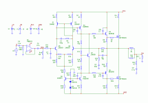
Are the zeners directly on the FET gate or are they before R24 & R26. I ask this beacuse if the zener on the positive side of the amp ever turned on, it will likely destroy T9. If the zener is directly on the gate you should increase R24 & R26 to 100 ohms to give the zener half a chance of doing its job.
So its a problem choice, the zener will provide a degree of over current protection, but will need some current limiting via a series resistance.
Cheers
Quasi
PS. Ahem.... it would be nice to see some builds from other constructors
This is truly a marvelous looking stereo amplier, congratulations.
Are the zeners directly on the FET gate or are they before R24 & R26. I ask this beacuse if the zener on the positive side of the amp ever turned on, it will likely destroy T9. If the zener is directly on the gate you should increase R24 & R26 to 100 ohms to give the zener half a chance of doing its job.
So its a problem choice, the zener will provide a degree of over current protection, but will need some current limiting via a series resistance.
Cheers
Quasi
PS. Ahem.... it would be nice to see some builds from other constructors
Quasi, the fuse placement in the Nmos amps (except the 400 which looks right) may cause a chain reaction destruction when the fuses blow. The drivers will try to drive the output on their own possibly punching through the gates of the output transistors and smoking their emitter resistors. If the gates of the outputs short or are zener protected the driver transistors will probably blow up too. The connection in the Nmos400 with drivers connected after fuses looks right but I suggest you add something to current limit the VAS too, for example clamping diodes or a zener between its base and the positive rail. As it is now the only thing limiting the VAS current when the output is unpowered and/or shorted is the current gain of the VAS and tail current of the input stage.
I've seen an amp blow up its drivers, VAS transistor and set some resistors on fire because of a bad connection on an output transistor emitter resistor - quite similar to having your rail fuses open in this design. One driver shorted as it tried to drive the output by itself and the non-current-limited VAS blew up trying to pull on the base of the shorted transistor. The resistors that burned were driver base resistors and VAS emitter resistor IIRC.
I've seen an amp blow up its drivers, VAS transistor and set some resistors on fire because of a bad connection on an output transistor emitter resistor - quite similar to having your rail fuses open in this design. One driver shorted as it tried to drive the output by itself and the non-current-limited VAS blew up trying to pull on the base of the shorted transistor. The resistors that burned were driver base resistors and VAS emitter resistor IIRC.
Hi Megajocke
Your point is quite valid and this part needs to be re-designed. It is easy to fix by putting all the amp circuitry after the fuse. This will have a slight affect on the performance however.
I have promised an Nmos series II for some time now, maybe it's time to deliver.
Cheers
Quasi
Your point is quite valid and this part needs to be re-designed. It is easy to fix by putting all the amp circuitry after the fuse. This will have a slight affect on the performance however.
I have promised an Nmos series II for some time now, maybe it's time to deliver.
Cheers
Quasi
Putting the input stages after the fuse has one drawback I can see - if the positive rail fuse blows the output will go to the negative rail. The connection used in the Nmos400 looks fine, adding a clamp for the VAS base should make the VAS stage protected from blown fuses and blown output stage/drivers.
I was looking for an amp to power my subwoofer. I have seen from previous posts that the nmos350 amp would be suitable for that.
I have not built any amp before. Would this amp be difficult to build if it is a first time build ? Will just following the schematics exactly allow a sucessful build ?
Thankz.
I have not built any amp before. Would this amp be difficult to build if it is a first time build ? Will just following the schematics exactly allow a sucessful build ?
Thankz.
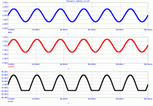
Hi, I'm up to build a couple of those amps for bridge operation. But I've encountered some issue. Amp didn't work properly with buffer, there is strong offset of input signal after buffer or inverter stage. It's on the picture. What's the case? I can't figure it out. How to fix it? Really want to bridge them ")
Attachments
Buzzy said:I was looking for an amp to power my subwoofer. I have seen from previous posts that the nmos350 amp would be suitable for that.
I have not built any amp before. Would this amp be difficult to build if it is a first time build ? Will just following the schematics exactly allow a sucessful build ?
Thankz.
This should not be your first electronics project. It can be your first amp project but you should have successfully completed other electronic projects of medium complexity. It might pay you to practice with a chip-amp first and get the feel of building a complete amp with power supplies, mains wiring etc.
Cheers
Q
niroborn said:Hi, I'm up to build a couple of those amps for bridge operation. But I've encountered some issue. Amp didn't work properly with buffer, there is strong offset of input signal after buffer or inverter stage. It's on the picture. What's the case? I can't figure it out. How to fix it? Really want to bridge them
Hmm...I don;t know what the problem is. Is there a DC offset being created on the base of the power amps input transistor?
Can anyone else help?
Cheers
Q
Quasi in Phuket
Hi Folks,
I will be away for about 7 days attending a conference in Phuket -Thailand. Please don't feel sorry for me, I had it coming. Of course if any fellow DIY'ers happen to be in Phuket over the next week send me an email and I'll give you some details. There will not be any posts from me during this time.
Try not to burn yourselves with your soldering irons and I'll try not to burn myself in the sun.
Cheers
Q
Re: Quasi in Phuket
Have a good trip, cheers
Hari
Quasi, do take some time out from the beach to attend the conferencequasi said:Hi Folks,
I will be away for about 7 days attending a conference in Phuket -Thailand. Please don't feel sorry for me, I had it coming. Of course if any fellow DIY'ers happen to be in Phuket over the next week send me an email and I'll give you some details. There will not be any posts from me during this time.
Try not to burn yourselves with your soldering irons and I'll try not to burn myself in the sun.
Cheers
Q
Have a good trip, cheers
Hari
Originally posted by quasi Hmm...I don;t know what the problem is. Is there a DC offset being created on the base of the power amps input transistor?
Yeah, there is apparently DC in the base of input transistor. Without buffer or inverter there is no DC. Buffer works great with other (Holton's) amplifier.
Please someone help, I've stuck on this.
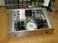
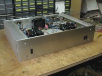
Maci.laci your amp looks so neat and compact.
I intend to use IRFP240 for the output instead of the irfp450. I have seen that Quasi has mentioned that irfp240 can be used in previous posts. Would I need to make any changes to the nmos350 circuit to use irfp240 ? Or can I just follow the schematic w/o changes ?
Thankz.
I intend to use IRFP240 for the output instead of the irfp450. I have seen that Quasi has mentioned that irfp240 can be used in previous posts. Would I need to make any changes to the nmos350 circuit to use irfp240 ? Or can I just follow the schematic w/o changes ?
Thankz.
Buzzy said:
I intend to use IRFP240 for the output instead of the irfp450. I have seen that Quasi has mentioned that irfp240 can be used in previous posts. Would I need to make any changes to the nmos350 circuit to use irfp240 ? Or can I just follow the schematic w/o changes ?
Thankz.
Yes you can. I used IRFP260N with no problem.
Hi,
one could have one timer/delay circuit controlling one relay shorting out one resistor, but feeding multiple transformers.
But, better would be one timer controlling dual relays, shorting dual resistors so that each transformer has the correctly selected series resistor.
one could have one timer/delay circuit controlling one relay shorting out one resistor, but feeding multiple transformers.
But, better would be one timer controlling dual relays, shorting dual resistors so that each transformer has the correctly selected series resistor.
- Home
- Amplifiers
- Solid State
- Power amp under development