Show us your sims! Present them for peer review!
If we accept your model, there are no loads which confound it. If we accept Different Cdyne Zouts, there are no loads which confound it. So what?
I challenge you to find any loads which confound diff Z. Will you accept that challenge? Good for the goose...
The problem is that your model is wrong, and you refuse to discuss why it is wrong. That is the real problem.
And so your model produces the wrong answers with all loads. So it is irrelevant what it does if you accept that it is true.
As for what you can't help that I don't understand - Oh, please!
Dave has shown the sims again and again.
When you present a pair of loads for which my model gives an incorrect experimental answer, I will be happy to engage you. If you are unable to experimentally verify your suggested exception, but are convinced by your modeling or calculation, I will be happy to do those measurements for you.
I've never said that a differential z model was wrong, so you're arguing with someone other than me.
You are missing what was stated in post 673. Please re-read it.
The impedance of a pair of nodes is the change in voltage (plate to ground) across the nodes due to the currents applied across those same nodes. The contribution to a voltage (plate) from a current applied to another node (cathode) does not figure in to the impedance at the plate.
consider a typical resistor loaded tube stage in which bias is supplied by a series resistor in the cathode.
your position must be that the "plate impedance" will not change if a capacitor is placed across the cathode resistor.
My position is that the bypass capacitor will change the circuit drastically.
dave
If Dave has shown it time and time again, then did you really run the sims? Show us your sims! You still haven't made the case that there is any flaw in post 673, where I have proven that Cdyne outputs have different impedances.
My answer to your confounding loads is above. But you keep ignoring it. And you ignore the challenge to find loads that confound the Cdyne model with different Zouts. How can you justify that when you demand it for your own model?
And you continue to ignore the demonstration using a current mirror that equal voltages across identical loads do not demand to be driven by sources of equal impedance, the opposite of which was a key argument in your article for equal Zout.
In fact, you continue to ignore the vast majority of challenges to your model that have been posted here.
Please explain how you don't consider the Diff_z Cdyne model, which claims different output impedances for a Cdyne, does not conflict with your claim that Cdyne output impedances are equal.
In response to post 704, Dave, that is not and never has been my position.
Where are you getting this? The current in the quote referred to a current source. A current source has infinite impedance. An independent current source can never affect the impedance of any point in a circuit.
Where are you getting this? The current in the quote referred to a current source. A current source has infinite impedance. An independent current source can never affect the impedance of any point in a circuit.
Stuart, post 673 has proven that Cdyne output impedances are different. Therefore, nothing can prove that they are equal - even matched load pairs. Therefore, all matched load pairs confound your model, and your challenge is met.
The challenge is now with you to refute 673.
The challenge is now with you to refute 673.
Unfortunately, experimental results and sims show that my model gives correct predictions. If by "your answer" you mean two AC current sources of opposite polarity, I do not have a pair of AC current sources on hand, though I will take the trouble to build them and try your guess at a pair of loads for which my model will give incorrect results IF:
1. You accept that if voltages measured at plate and cathode are low (i.e. ~2I/gm) and equal, my model give correct predictions and works, and...
2. you then stop demanding that I take the time and effort to go through your more complex model to either find defects or show how it agrees with mine in all cases of the "equal loads" constraint (you're free to do so if you want).
On the other hand, if the experimentally observed voltages are different and/or high, or for whatever reason do not agree with the predictions of my model, I'll discard it and apologize publicly for my stubborn misunderstanding.
That's my final word on this.
Stuart, let me save you some trouble. There is no need for you to build anything.
You have a flaw in (1) above. It seems that you are unaware that equal voltages and equal impedances are not the same thing.
I have tried to get you to fulfill your promise to respond to the current mirror, but you have yet to do so. If you like simplicity, you'll like this one - there are no equations involved, and so it is simpler than your model. Let me repeat it here for convenience.
Drive the input of a unity gain mirror from a voltage source through an impedance Z, and terminate its output in an identical Z. Since the gain is unity, both Z's see the same current and so by Ohm's law, both Z's develop the same voltage.
Now if you are unfamilair with a simple current mirror, check out File:Simple bipolar mirror.svg - Wikipedia, the free encyclopedia . By inspection of figure 1, it is clear that the base emitter junction of the input has a much lower impedance than the reverse biased output of the collector (the high output impedance is even mentioned in the wiki.)
The implications are significant. Very different source impedances produce equal voltages across identical loads. Equal voltage does NOT imply equal impedance. The consequence for the Cdyne is clear - you are simply not justified in using equal voltages to conlude equal impedances, as you did in your article.
If I can only get you to understand this...
You have a flaw in (1) above. It seems that you are unaware that equal voltages and equal impedances are not the same thing.
Shorter Chris: I still don't have a matched pair of loads where SY's model gives an incorrect result. When you do, get back to me and my offer still stands.
Stuart, you have a very bad understanding of language if that is what you get from the quote.
Post 673 has answered your challenge. Falsify it, or ratify it. Deal with it. It confirms that all loads confound your model. Do you have the engineering background to understand the point that it makes?
In your refusal to even acknowledge, let alone discuss, the simple example of the current mirror and its implications to your understanding of the Cdyne, and in your insistence on discussing solely your matched loads, you exhibit behavior that can only be described as intellectual arrogance. I would not point this out if you hadn’t consistently ignored arguments presented over the past several hundred posts, but I think the facts are clear. I know you're better than that, but that's how you're behaving.
In any discussion between people who are honestly engaged in finding the truth, no one person gets to control the agenda of the discussion. All ideas need to be considered and vetted. Or do you disagree?
Think about it.
I'm sorry to see you once again disengage.
Dave, have you simulated the expession I gave you in post 701 to predict Cdyne bandwidth?
Not sure what you are asking. I have loaded down the Cdyne with capacitive loads and the bandwidth matched the expected roloff of a fixed source driving a capacitive load.
dave
I believe some of the controversy over this topic results from imprecise terminology. I see terms like "apparent impedance", "ficticious impedance", "output impedance", etc., and just "impedance" without any qualifier. Since about 1929 when Feldtkeller in Germany began using matrix algebra for network analysis, there have been several well defined terms in use.
The IEEE Dictionary of electrical terms defines impedance, as it applies to passive networks, like this (not an exact quote):
Inject a current into a node of a network and measure the voltage thus produced at that node. Divide the voltage by the current. This is the driving point impedance.
Inject a current into a node of a network and measure the voltage thus produced at some other node. Divide the voltage by the current and this is the transfer impedance to the other node.
I see various indirect methods used to determine the "output" impedance of the Cathodyne. One such method is being used beyond its range of applicability.
A common technique for calculating (or measuring) "output" impedance (which is typically a driving point impedance) is to use the voltage divider method. A signal is applied to an input node of the network and the unloaded open circuit voltage is measured at an "output" node. Then a load (resistor) is connected to the output node and it is adjusted until the loaded output voltage decreases by half. The load resistor is disconnected and measured. Its value is taken to be the "output" impedance. This procedure can be misleading at times.
In what follows, when I say "impedance", or "output impedance", I will mean a driving point impedance unless otherwise specified. Sometimes I may say "driving point" explicitly to avoid possible ambiguity.
Consider the following resistor network. It has 3 nodes and 4 resistors.
We'll apply a voltage to node 1 and measure the output voltages at nodes 2 and 3. The ratio of the voltage at node 2 or 3 to the voltage at node 1 will be called the gain to that output node. (Strictly, it should be called the open circuit voltage transfer ratio.) Since this network is intended to be driven by a voltage source, we must ground node 1 when calculating (or measuring) the output impedance at node 2 or 3.
Let's apply 1 volt to node 1 and calculate the voltages at nodes 2 and 3. The output voltage would be 2/6 or .3333333333 volts. The gain is 1/3 to both nodes 2 and 3.
Ground node 1 and calculate the driving point resistance at nodes 2 and 3. It's 2||4 ohms, or 1.33333333 ohms. Now let's apply some additional load at nodes 2 and 3, sufficient to reduce the gain to 1/2 its previous value. One would think that a resistor equal to the output resistance of the network would do the job. So, connect a 1.33333333 ohm resistor in parallel with each of the 2 ohm resistors, and calculate the gain to nodes 2 and 3. It's .166666667, which is indeed half the value without the added resistors.
Now consider this network:
It's the same as the first one except for the additional 4 ohm resistor between nodes 2 and 3.
The output (driving point) resistance at nodes 2 and 3 separately is 1.066666667 ohms. Don't forget to ground node 1 when making this calculation.
The voltage gain from node 1 to nodes 2 and 3 is .3333333333. This is to be expected since the additional 4 ohm resistor is connected between two nodes that have the same voltage when a source is driving node 1; it draws no current and has no effect on the output voltage.
What additional loads applied to nodes 2 and 3 will cause the gain to those nodes to be 1/2 of its previous value? One might think that it would simply be resistors equal to the output resistance. Let's try it. Add a 1.06666667 ohm resistor from node 2 and node 3 to ground, and calculate the gain to those nodes. The result is a gain of .148148148. But we expected a gain of .166666667; what went wrong?
The problem is that there is coupling between nodes 2 and 3 due to the 4 ohm resistor we added. If we go back to Network 1 and imagine injecting some current into node 2 and measuring the voltage produced at node 3 (remember, node 1 must be grounded for these measurements), we can easily see that there will be none. In other words, the transfer impedance is zero; there is no coupling between nodes 2 and 3.
Do the same with Network 2; ground node 1, inject 1 amp into node 2 and calculate the voltage produced at node 3. The result is .266666667 volts, and since 1 amp was injected, the transfer resistance is .266666667 ohms. Does this help us find the load which will reduce the voltage gain by 1/2? Yes. The required load is the sum of the driving point impedance and the transfer impedance. So, connect a 1.3333333 ohm resistor from nodes 2 and 3 to ground and calculate the voltage gains to nodes 2 and 3. The result is a gain of .166666667, which is half the gain without the additional load.
One could have noticed that because of the extreme symmetry of the circuit, the additional 4 ohm resistor doesn't affect the gains. But it does change the output (driving point) resistance at nodes 2 and 3 (as determined separately), so from one point of view it's clear that the same load resistance that we used with Network 1 will also work with Network 2. But, we also have been told that load resistors equal to the output resistance should reduce the gain by half, which is not true for this network. Using the transfer resistance leads us back to the correct loads.
A differential output resistance of Network 1 could be measured by connecting an ohmmeter between nodes 2 and 3. If this is done, the ohmmeter will inject a current I into one of nodes 2 or 3, extract a current I from the other node and measure the voltage between the nodes(extracting a current I from a node is the same as injecting a current -I into that node). The voltage between the nodes divided by the current I gives the differential resistance.
It's easy to see that the differential output resistance of Network 1 is 2.66666667 ohms, and of Network 2 is 1.6 ohms. Adding the extra (differentially connected) 4 ohm resistor in Network 2 changed the differential output resistance, changed the driving point output resistances, but did NOT change the load resistances necessary to multiply the voltage gains to nodes 2 and 3 by 1/2.
We calculated output (driving point) resistances of 1.06666667 ohms for Network 2; why did we need loads of 1.3333333 ohms to reduce the gain by half? With Network 1, the required load was equal to the calculated output (driving point) resistance but not with Network 2. Does this mean that the output resistance of Network 2 changes to 1.33333333 ohms when we add two loads instead of just one?
No. The problem is that the classical voltage divider formula only works for one output at a time. In fact, if you add a 1.066666667 ohm resistor from node 2 to ground in Network 2 (but not from node 3 at the same time) and calculate the gain to node 2, it will be .166666667, half the previous value. The 1.33333333 ohm value is not an output impedance; it is the sum (it would be the difference if one of the gains had a negative sign) of the output impedance and the transfer impedance. It is a number which will give you the voltage gain when used where you shouldn't use it, in the voltage divider formula (applied to 2 nodes at a time), which is only guaranteed valid for one output at a time. We can see that the voltage divider formula, using the actual output impedance, is not ALWAYS valid when used for more than one output at a time. It is invalid when the network has non-zero transfer impedances connecting the nodes in question. In that case we can derive a another number (which is not the output impedance) which will work in the voltage divider formula for two outputs at a time (when I say it will "work" I mean that it will reduce the voltage to a node by 1/2 when applied as a load). But this does not mean that the number is the output impedance of the network. Some might be tempted to call it an "apparent" output impedance. And, of course, the only time one such number will work for two outputs simultaneously is when the network has a high degree of symmetry, like Network 2.
Network theory teaches that passive networks like these are completely characterized by their driving point impedances (this is what would normally be meant by the term output impedance) and their transfer impedances.
Unfortunately, I think, even though this procedure is not mathematically valid for networks that have a non-zero transfer impedance between two nodes under scrutiny, it nonetheless works for the Cathodyne, which does have non-zero transfer impedances between plate and cathode. I will demonstrate this happenstance in further posts.
The IEEE Dictionary of electrical terms defines impedance, as it applies to passive networks, like this (not an exact quote):
Inject a current into a node of a network and measure the voltage thus produced at that node. Divide the voltage by the current. This is the driving point impedance.
Inject a current into a node of a network and measure the voltage thus produced at some other node. Divide the voltage by the current and this is the transfer impedance to the other node.
I see various indirect methods used to determine the "output" impedance of the Cathodyne. One such method is being used beyond its range of applicability.
A common technique for calculating (or measuring) "output" impedance (which is typically a driving point impedance) is to use the voltage divider method. A signal is applied to an input node of the network and the unloaded open circuit voltage is measured at an "output" node. Then a load (resistor) is connected to the output node and it is adjusted until the loaded output voltage decreases by half. The load resistor is disconnected and measured. Its value is taken to be the "output" impedance. This procedure can be misleading at times.
In what follows, when I say "impedance", or "output impedance", I will mean a driving point impedance unless otherwise specified. Sometimes I may say "driving point" explicitly to avoid possible ambiguity.
Consider the following resistor network. It has 3 nodes and 4 resistors.
Code:
[FONT="Fixedsys"]
                Network 1

      2     ___    1      ___    3
      .----|___|---.-----|___|---.
      |      4     |       4     |
      |           In             |
     .-.                        .-.
     | |                        | |
    2| |                        | |2
     '-'                        '-'
      |                          |
      -------------.--------------
                   |
                  GND[/FONT]
We'll apply a voltage to node 1 and measure the output voltages at nodes 2 and 3. The ratio of the voltage at node 2 or 3 to the voltage at node 1 will be called the gain to that output node. (Strictly, it should be called the open circuit voltage transfer ratio.) Since this network is intended to be driven by a voltage source, we must ground node 1 when calculating (or measuring) the output impedance at node 2 or 3.
Let's apply 1 volt to node 1 and calculate the voltages at nodes 2 and 3. The output voltage would be 2/6 or .3333333333 volts. The gain is 1/3 to both nodes 2 and 3.
Ground node 1 and calculate the driving point resistance at nodes 2 and 3. It's 2||4 ohms, or 1.33333333 ohms. Now let's apply some additional load at nodes 2 and 3, sufficient to reduce the gain to 1/2 its previous value. One would think that a resistor equal to the output resistance of the network would do the job. So, connect a 1.33333333 ohm resistor in parallel with each of the 2 ohm resistors, and calculate the gain to nodes 2 and 3. It's .166666667, which is indeed half the value without the added resistors.
Now consider this network:
Code:
[FONT="Fixedsys"]                Network 2
                  ___
        ---------|___|----------
        |          4           |
        |                      |
        |                      |
      2 |   ___     1     ___  | 3
      .-'--|___|---.-----|___|-'-.
      |      4     |       4     |
      |           In             |
     .-.                        .-.
     | |                        | |
    2| |                        | |2
     '-'                        '-'
      |                          |
      -------------.--------------
                   |
                  GND[/FONT]
It's the same as the first one except for the additional 4 ohm resistor between nodes 2 and 3.
The output (driving point) resistance at nodes 2 and 3 separately is 1.066666667 ohms. Don't forget to ground node 1 when making this calculation.
The voltage gain from node 1 to nodes 2 and 3 is .3333333333. This is to be expected since the additional 4 ohm resistor is connected between two nodes that have the same voltage when a source is driving node 1; it draws no current and has no effect on the output voltage.
What additional loads applied to nodes 2 and 3 will cause the gain to those nodes to be 1/2 of its previous value? One might think that it would simply be resistors equal to the output resistance. Let's try it. Add a 1.06666667 ohm resistor from node 2 and node 3 to ground, and calculate the gain to those nodes. The result is a gain of .148148148. But we expected a gain of .166666667; what went wrong?
The problem is that there is coupling between nodes 2 and 3 due to the 4 ohm resistor we added. If we go back to Network 1 and imagine injecting some current into node 2 and measuring the voltage produced at node 3 (remember, node 1 must be grounded for these measurements), we can easily see that there will be none. In other words, the transfer impedance is zero; there is no coupling between nodes 2 and 3.
Do the same with Network 2; ground node 1, inject 1 amp into node 2 and calculate the voltage produced at node 3. The result is .266666667 volts, and since 1 amp was injected, the transfer resistance is .266666667 ohms. Does this help us find the load which will reduce the voltage gain by 1/2? Yes. The required load is the sum of the driving point impedance and the transfer impedance. So, connect a 1.3333333 ohm resistor from nodes 2 and 3 to ground and calculate the voltage gains to nodes 2 and 3. The result is a gain of .166666667, which is half the gain without the additional load.
One could have noticed that because of the extreme symmetry of the circuit, the additional 4 ohm resistor doesn't affect the gains. But it does change the output (driving point) resistance at nodes 2 and 3 (as determined separately), so from one point of view it's clear that the same load resistance that we used with Network 1 will also work with Network 2. But, we also have been told that load resistors equal to the output resistance should reduce the gain by half, which is not true for this network. Using the transfer resistance leads us back to the correct loads.
A differential output resistance of Network 1 could be measured by connecting an ohmmeter between nodes 2 and 3. If this is done, the ohmmeter will inject a current I into one of nodes 2 or 3, extract a current I from the other node and measure the voltage between the nodes(extracting a current I from a node is the same as injecting a current -I into that node). The voltage between the nodes divided by the current I gives the differential resistance.
It's easy to see that the differential output resistance of Network 1 is 2.66666667 ohms, and of Network 2 is 1.6 ohms. Adding the extra (differentially connected) 4 ohm resistor in Network 2 changed the differential output resistance, changed the driving point output resistances, but did NOT change the load resistances necessary to multiply the voltage gains to nodes 2 and 3 by 1/2.
We calculated output (driving point) resistances of 1.06666667 ohms for Network 2; why did we need loads of 1.3333333 ohms to reduce the gain by half? With Network 1, the required load was equal to the calculated output (driving point) resistance but not with Network 2. Does this mean that the output resistance of Network 2 changes to 1.33333333 ohms when we add two loads instead of just one?
No. The problem is that the classical voltage divider formula only works for one output at a time. In fact, if you add a 1.066666667 ohm resistor from node 2 to ground in Network 2 (but not from node 3 at the same time) and calculate the gain to node 2, it will be .166666667, half the previous value. The 1.33333333 ohm value is not an output impedance; it is the sum (it would be the difference if one of the gains had a negative sign) of the output impedance and the transfer impedance. It is a number which will give you the voltage gain when used where you shouldn't use it, in the voltage divider formula (applied to 2 nodes at a time), which is only guaranteed valid for one output at a time. We can see that the voltage divider formula, using the actual output impedance, is not ALWAYS valid when used for more than one output at a time. It is invalid when the network has non-zero transfer impedances connecting the nodes in question. In that case we can derive a another number (which is not the output impedance) which will work in the voltage divider formula for two outputs at a time (when I say it will "work" I mean that it will reduce the voltage to a node by 1/2 when applied as a load). But this does not mean that the number is the output impedance of the network. Some might be tempted to call it an "apparent" output impedance. And, of course, the only time one such number will work for two outputs simultaneously is when the network has a high degree of symmetry, like Network 2.
Network theory teaches that passive networks like these are completely characterized by their driving point impedances (this is what would normally be meant by the term output impedance) and their transfer impedances.
Unfortunately, I think, even though this procedure is not mathematically valid for networks that have a non-zero transfer impedance between two nodes under scrutiny, it nonetheless works for the Cathodyne, which does have non-zero transfer impedances between plate and cathode. I will demonstrate this happenstance in further posts.
Continuing the discussion.
Starting with Feldtkeller, network analysis has been systematized by the use of matrix algebra. Two common methods of network analysis are the nodal method and the loop method. The nodal method leads to a matrix of admittances, the Y matrix. The loop method leads to a matrix of impedances, the Z matrix.
A general Y matrix is often shown like this:
[ y11 y12 y13 ]
[ y21 y22 y23 ]
[ y31 y32 y33 ]
The number of rows and columns in a Y matrix correspond to the total number of nodes-1 in a network. One of the network nodes is taken to be the reference node, usually circuit ground, so a 3x3 matrix will represent a network with 4 nodes, one of which is ground. It is customary to assume ground is the reference node, so it isn't counted when we say that a 3x3 matrix represents a 3 node network; the reference node is assumed and not mentioned.
I'll mainly be using a 3x3 matrix because the simple Cathodyne circuit has 3 nodes, as did the two networks I discussed in the previous post.
Modern mathematical programs, such as Mathematica and Maple can solve matrix equations, even with symbolic rather than numerical elements. This removes most of the drudgery from analysis of even rather complicated networks. There are also free programs such as Scilab and Maxima that can do the job. Even some modern hand held calculators can do symbolic matrix algebra, such as the HP50G and TI89.
In November of 1952, Jacob Shekel published a paper in the Proceedings of the IRE describing how to use matrix methods to analyze transistor circuits; the same methods apply to vacuum tubes as well. I'll be using some of his techniques. I explain the methods starting at post #43 of this thread:
Two stage BJT amplifier with feedback - All About Circuits Forum
The two attached images show how to form the Y (admittance) matrix for Network 1 and Network 2 from the previous post. Then several properties of the networks are derived using matrix algebra and Shekel's method with Mathematica.
The attached images are .png files and are rather tall. They can be conveniently viewed with Firefox. Position the cursor over the image and you should see a tiny magnifying glass. Left click and you'll see the full size image and you can scroll up and down.
Attachments
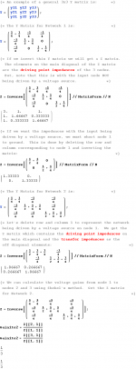
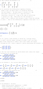
The attached images show the Y matrix for the Cathodyne and the results of manipulating it with matrix algebra in Mathematica.
This technique allows one to derive any property of the circuit rather easily. The drudgery of substantial symbolic algebra is taken care of by the computer.
To find the driving point impedances at the plate and cathode one need only invert the admittance matrix.
The impedance for balanced loads is the differential impedance which is also easily derived as shown.
This method of analysis automatically takes care of the case where the loads are not perfectly balanced. Whatever the loads are equal or not, slightly unbalanced or greatly unbalanced, the analysis will be correct. There's no need to resort to "apparent" impedances, or the like.
I show a somewhat complicated expression for load resistors (Ra and Rb in the images) that will reduce the voltage gain by 1/2, and I show that this gives exactly the same result as the calculation of the differential impedance. This is only true for a circuit whose Y matrix has substantial symmetry is the lower right 2x2 submatrix, which the Cathodyne does.
I'll show the effects of unbalance due to stray capacitance in later posts.
Attachments
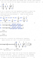
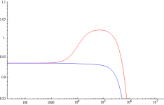
The attached image shows the voltage gain vs. frequency for the Cathodyne in SY's article in Linear Audio with 1000 pF shunted to ground from the plate and 1100 pF shunted to ground from the cathode.
This is the difference in response caused by a 10% unbalance in capacitance loading. I used relatively large capacitance to get the lowest corner frequency just into the audio band.
The red curve is the response at the plate and the blue curve is the cathode response.
This result was obtained with Shekel's method and the Y matrix for the Cathodyne from the previous post.
Attachments
- Status
- This old topic is closed. If you want to reopen this topic, contact a moderator using the "Report Post" button.
- Home
- Amplifiers
- Tubes / Valves
- phase splitter issue