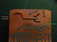
I worked a bit, and came up with what seems to be my final implementation of my pcb.
I will use the idea of point-to-point live wire from fuse to primary. Plus, I drilled some openings through the pcb, so that I will increase creepage, using an 1.2mm HSS drill. These openings were made as "barriers" between the solder joints and traces of interest. The result is the following:

Now creepage is defined around the openings, so that at a minimum it is at least 10mm, as I roughly measured. Surely above 8mm. And corresponding minimum air clearance is 7mm.
So it seems like the pcb is already fine! Maybe I will also paint live and neutral traces too, or involve any plastic shielding like discussed before - but hopefully, this will be to my liking and boredom - the icing on the cake!
Thank you all for your kind and detailed responses. I learned some things today, and hopefully designed my pcb the right way. Certainly way better than it was in the beginning.
I will use the idea of point-to-point live wire from fuse to primary. Plus, I drilled some openings through the pcb, so that I will increase creepage, using an 1.2mm HSS drill. These openings were made as "barriers" between the solder joints and traces of interest. The result is the following:

Now creepage is defined around the openings, so that at a minimum it is at least 10mm, as I roughly measured. Surely above 8mm. And corresponding minimum air clearance is 7mm.
So it seems like the pcb is already fine! Maybe I will also paint live and neutral traces too, or involve any plastic shielding like discussed before - but hopefully, this will be to my liking and boredom - the icing on the cake!
Thank you all for your kind and detailed responses. I learned some things today, and hopefully designed my pcb the right way. Certainly way better than it was in the beginning.
Isn't this all becoming a bit overcautious ? Well it isn't a question but more a fact. It still is a 230 V AC mains fed low power device isn't it ? You are not dealing with 10 kV or stuff like that. Stay with both feet on the ground.
You don't live in the UK/US otherwise you would also need a "certified" inspector wearing safety goggles + gloves, a safety mask and using an insulating mat to plug it in mains ...Don't forget to use tape "to secure the perimeter". Don't forget the LOTO procedure and try to make everybody scared of all the possible risks. Show videos of situations elsewhere where things went horribly wrong. Document all the possible risks and have them reviewed by agencies beforehand. Let assurance company come over and pay extra for the documented risks.
You don't live in the UK/US otherwise you would also need a "certified" inspector wearing safety goggles + gloves, a safety mask and using an insulating mat to plug it in mains ...Don't forget to use tape "to secure the perimeter". Don't forget the LOTO procedure and try to make everybody scared of all the possible risks. Show videos of situations elsewhere where things went horribly wrong. Document all the possible risks and have them reviewed by agencies beforehand. Let assurance company come over and pay extra for the documented risks.
Last edited:
Jean-paul,
I agree that this is overcautious. But being young, I want to start becoming familiar with safety practices, that could be useful some day. Besides, I don't think I lost anything - a bit of time and only that: the final design costs as much as the first, and will not make me lose any sleep - not that 3mm spacing would (it could, given my lack of knowledge), but for sure, the first design was a bit weird I would say. 1.7mm spacing when you can easily get more is bad practice in my view. And I corrected myself, with everyone's aid, including you. Learned through that experience.
Maybe through your experienced eyes all this is boring, but for me, it is a small gain in my engineering knowledge!
And, remember, the final point isn't actually that I strived and succeeded in making clearance and creepage more than 7mm - it is the fact that all these considerations were brought to my attention through this forum. At the end of the day I did the best I could (maybe this best is not necessary, I agree), but I view it more like a prize for the effort of this day.

Learning of course is good but nowadays things get very exaggerated when safety is concerned just because it is booming business. Point is that fear is used to make us all aware that it is very important. Safety IS important but most of the time money is the motivation.
Try to make things good straight when you start a project as it will save you time and frustration. Don't take things for granted. Then make the design better by looking with other eyes (or let other people have a look !) to your own design, change matters accordingly and ...stop when it is on the verge of becoming "too good".
Hey, hobby stuff is never boring ! You can carry on for tens of pages on this subject if you like.
Last edited:
I earlier asked for peoples comments on spacing on PCB inner layers, I did this for a purpose, (no reply's SOB). The reason being is that even in my world of pain (PCB design) I get different requirements from different engineers regarding the same specification IEC-60950 depending on how they interpret the requirements. I spent 8 years laying out PCBs for Generator and mains control and measurement to full UL and CE compliance so have spent a lot of time looking at the specifications, and can say quite categorically that they are not easy to follow or determine the required spacing's.
For your designs Audiostrat pollution level 2 is the correct level, I will try and dig through my documentation and try and find a simplified breakdown of IEC-60950 that a few of us worked on several years ago.
On the PCB side, inner layer spacing's are.............
For your designs Audiostrat pollution level 2 is the correct level, I will try and dig through my documentation and try and find a simplified breakdown of IEC-60950 that a few of us worked on several years ago.
On the PCB side, inner layer spacing's are.............
Last edited:
When your house burns down and your insurance company become aware that you dabble in home built mains powered projects, I would not be surprised if the insurance company instructed the surveyor to find "any" non compliant practice that would allow them to pay out nothing.
If the fire resulted in a death, I suspect the Police would also become involved in finding any evidence of culpability.
Beware of belittling "Safety".
If the fire resulted in a death, I suspect the Police would also become involved in finding any evidence of culpability.
Beware of belittling "Safety".
Last edited:
When your house burns down and your insurance company become aware that you dabble in home built mains powered projects, I would not be surprised if the insurance company instructed the surveyor to find "any" non compliant practice that would allow them to pay out nothing.
That's what they always do even when there are no home built mains powered projects around. Insurance companies make it a habit to find matters to pay less than required or nothing at all.
Beware of belittling "Safety".
Also beware of exaggerating. Please check where most incidents occur....
- Status
- This old topic is closed. If you want to reopen this topic, contact a moderator using the "Report Post" button.
- Home
- Amplifiers
- Power Supplies
- pcb safety spacing