Don't be afraid, I won't get married for that pcb. 
Well, my first post is post 11, and as you can see my first phrase is just that!
This is the whole point, live to neutral. The link dealing with creepage.com suggested that 1.0mm is functional for this, the way I understood it.
I can change the pcb, in that I could repaint the live wire and keep it at a greater distance from the neutral solder pad (see attachment), before I etch it. But this would mean that it will get closer to the secondary traces.
So, what is the minimum clearance I would allow between live and secondary? 230V mains. If it is, say, 8mm, I can allow 8mm between live/secondary, and so 3.7mm between live/neutral. Would this be adequate?
Secondary voltage could rise up to 21.25 VAC (according to specs of the pcb transformer), if mains is at 110%. So, 30VDC peak voltage.
Last edited:
That is adequate IMO. Please draw the footprint of a 2 pin Phoenix MKDSN-1.5 connector for 230 V AC input when you will the change the PCB anyway.
https://www.phoenixcontact.com/online/portal/us?uri=pxc-oc-itemdetail:pid=1729128&library=usen&tab=1
I am sure you will like that. Way safer than soldered 230 V carrying wires and servicing will be easier. When soldering relatively thick copper wire to PCB's the slightest mechanical force will peel the 230 V carrying PCB track off the PCB....If it's a power supply you could use the same connector at the output too. We used those for both purposes but changed over to Molex KK for low current output power supplies (at the output) as we then avoid the risk of people connecting stuff the wrong way around
Last edited:
You need at least 2.5mm between live and neutral, so your revised layout giving 3.7mm is more than adequate.
http://www.ce-mag.com/ce-mag.com/archive/01/03/ProductSafety.html
250V working, pollution degree 2, material group iii. I'm assuming your equipment is earthed.
http://www.ce-mag.com/ce-mag.com/archive/01/03/ProductSafety.html
250V working, pollution degree 2, material group iii. I'm assuming your equipment is earthed.
Last edited:
Jean-paul, I will use a clamp for the output voltage of this power supply. I initially planned to use one for mains too, but I decided that I would prefer for this application to hide any possible contact with mains, while pcb is at place. Next time! 
Richie00boy, my application will not be earthed. It is a plastic box, the type that plugs into the wall.
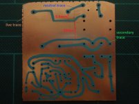
After some work, I got my new pcb design. Now, clearance of live/neutral is at least 3.4mm and live/secondary 10mm. Much better than before:
Richie00boy, my application will not be earthed. It is a plastic box, the type that plugs into the wall.
After some work, I got my new pcb design. Now, clearance of live/neutral is at least 3.4mm and live/secondary 10mm. Much better than before:

I use a thick plastic sheet on the back of any PCB that has high voltage on it.
This sheet is mechanically fixed in place.
Where there is Mains voltage I wrap that in red tape as a warning to dropped tools. "Don't fall here".
Similarly I now double wrap all my mains cabling in that same red tape.
Anyone opening up my box instantly sees where mains is !
This sheet is mechanically fixed in place.
Where there is Mains voltage I wrap that in red tape as a warning to dropped tools. "Don't fall here".
Similarly I now double wrap all my mains cabling in that same red tape.
Anyone opening up my box instantly sees where mains is !
Track spacing is an interesting one.
If you can GUARANTEE the spacing then air is a very poor conductor of electricity, unfortunately you have to allow for other factors such as leaching, condensation, dust and crud just to name a few.
That's covered by pollution levels in the relevant specs (IEC-60950 is one that comes to mind). For audio gear in a house I would say the lowest level (1) applies, as it is generally a benign atmosphere in a house, low condensation, dirt etc.
Woops level 2 for domestic, sorry.
Last edited:
Marce, a couple of things to specify:
(1) This will be a wall-plug power supply, to be used with an effects pedal. Which means it will mainly be inside a house or a studio, but could possibly travel to a gig place.
(2) I don't know about humidity levels and how these affect the choice, but currently we have 79% at home! We have also reached 85%.
(3) Pcb material is FR4: http://www.mgchemicals.com/products/prototyping-and-circuit-repair/copper-clad-boards/500-series/
About the wires going into the pcb? If I twist them and their insulation is rated for 300V, could I encounter any problems?
(1) This will be a wall-plug power supply, to be used with an effects pedal. Which means it will mainly be inside a house or a studio, but could possibly travel to a gig place.
(2) I don't know about humidity levels and how these affect the choice, but currently we have 79% at home!
(3) Pcb material is FR4: http://www.mgchemicals.com/products/prototyping-and-circuit-repair/copper-clad-boards/500-series/
About the wires going into the pcb? If I twist them and their insulation is rated for 300V, could I encounter any problems?
Last edited:
Insulation is a class 1 insulator so the distance goes down to 0.4mm as long as you are not going to damage the insulation.. I will have to dig out the specs and double check, we tend to use 4mm clearance and 8mm creepage then we are covered for every situation (the 8mm creepage can be reduced to 4mm if you have a slot of 1mm or greater between the conductive metal. When considering connectors the distance is from the edge of the pad to the next pad, solder resist does not count, you pretend it is not there.
Just out of interest I would be interested in peoples thoughts on gaps on inner layers of multi layer PCBs....
Oh and remember FR4 is used in very high voltage applications for separation of voltages,
Dielectric breakdown-A > 50 kV
Dielectric breakdown-D48/50 > 50 kV
Dielectric strength 20 kV/mm
Just out of interest I would be interested in peoples thoughts on gaps on inner layers of multi layer PCBs....
Oh and remember FR4 is used in very high voltage applications for separation of voltages,
Dielectric breakdown-A > 50 kV
Dielectric breakdown-D48/50 > 50 kV
Dielectric strength 20 kV/mm
Any covering is an aid, to cover equipment that satisfies all the specs you need conformal coatings and inspection etc of such, for DIY use AndrewT's solution is a good one, as you are not selling commercial gear (to sell stuff you need to get it CE or UL marked)
Once did a PSU with 35,000V x1 10,000V x 2 1,500V x10, now that was fun, 10mm polycarbonate outer casing with 20mm gap between that and the inner casing. Used on???
Once did a PSU with 35,000V x1 10,000V x 2 1,500V x10, now that was fun, 10mm polycarbonate outer casing with 20mm gap between that and the inner casing. Used on???
Then, how about soldering (using locktite glue) a small piece of 1.6mm FR4 between the two traces, acting as a "wall"? See attachment in post #25 to get the idea. Then I could raise creepage and clearance.
I must admit I did not quite understand your remark for the 1mm hole!
Yeah, where did you use that?
I must admit I did not quite understand your remark for the 1mm hole!
Yeah, where did you use that?
I cover the back (pcb trace side and component solder side with all those sharp ends ready to poke through a piece of thin insulating tape) to give a secure insulated surface that does not allow the traces to be touched, not even with a dropped tool.
0.5mm to 1mm thick tough plastic sheet. I keep my flat sided yoghurt containers for this. The lid is too thin.
0.5mm to 1mm thick tough plastic sheet. I keep my flat sided yoghurt containers for this. The lid is too thin.
Richie00boy, my application will not be earthed. It is a plastic box, the type that plugs into the wall.
In that case you need 5mm between live and earth as you are building an appliance with reinforced insulation (no portective earth requires reinforced insulation).
About the wires going into the pcb? If I twist them and their insulation is rated for 300V, could I encounter any problems?
As long as the insulation is 0.4mm or thicker it should be fine, preferably UL listed (says AWM style xxxx).
Well done for at least trying by the way.
Thanks, richie00boy.
How about the solution of adding an FR4 barrier between the two traces then? This should ensure that clearance is about 6mm at least.
As I also suggested, maybe I could solder (using glue) some wire insulation so that it would completely cover the live and neutral wires. What do you think?
EDIT: Or I could again try to make the distance larger, at the expense of reducing the live/secondary clearance to about 8mm. Would this be better than the above solution? I assume the best is a combination of this and the above.
Last edited:
One thing that came to mind: what if I actually used an insulated wire to make the connection of the live wire that is close to the neutral? (picture at post #25 will show what I mean). I mean, leaving only the pads where the pins of transformer and fuse will go, and soldering directly to them the wire.
Point to point, actually.
Would this ensure I am fully safe? Since you guys tell me that 0.4mm insulation is good enough!
Point to point, actually.
Would this ensure I am fully safe?
creepage distance is where the voltage can track over a surface so is longer than clearance, if you put a SLOT between two pads you can get away with the clearance distance, the slot has to be 1mm or wider to conform to IEC-60950.
If you use 8mm gap you will be covered for most if not all situations. One of the biggest problems is during the development and testing phase of design, when boards are usually on a bench being worked on, any measure you can take to avoid accidental touching of live parts is good practice.
If you use 8mm gap you will be covered for most if not all situations. One of the biggest problems is during the development and testing phase of design, when boards are usually on a bench being worked on, any measure you can take to avoid accidental touching of live parts is good practice.
Marce, thanks for the response. Sadly, I don't seem to have all that space to provide an 8mm gap.
I think that the solution of making the live wire an actual insulated wire would be quite adequate, based on everything you say for 0.4mm insulation. How about that? Quite simple, I think. If I don't make it clear enough, let me know so I provide a picture of what I mean.
I would like to ensure that no finger can touch a live connection, as long as the pcb stays in place. This will enable me to make measurements without being at peril (caution and common sense are always present, though).
Maybe I will also provide printed words for that. Good news is that you can't open the enclosure unless you first disconnect it from mains - so you will face the warning!
So I present my idea of using insulated wire instead of a pcb trace:
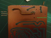
And covering the solder connections using wire insulation or even heatshrink tube - I have one that goes from 3.0mm to 1.5mm and says 600V on it - sounds good enough.
This way, actual live/neutral separation should be 10mm, where they enter the pcb.
So, how does that sound to clarify for reinforced?
- Status
- This old topic is closed. If you want to reopen this topic, contact a moderator using the "Report Post" button.
- Home
- Amplifiers
- Power Supplies
- pcb safety spacing
