Albert, I just got a chance to watch and listen to your scope video of the noise. Is the nose we are hearing on the video coming from speakers? Or is it coming form the relays mechanical switching noise?
Hi Bfpca,
Thanks for your help. The noise you hear is the clicking of the relays. I tested the RelVol3 board with a 1KHz square wave generator connected to the input of the RelVol3 board and an analog scope connected to the output of the RelVol3 board. The P1.7 amp board was not connected (not even powered during this test).
I understand that it will not be the smooth (infinite step) change I see with a pot, but I assume I should see a clean jump from 1 level to the next, without the distortion.You will get steps in the change in attenuation with this setup versus a pot.
I built a 23 step 25k shunt attenuator using a mechanical switch for my B1. When I turn the volume up or down in the B1 the sound gets louder or softer but does not distort. I will remove the attenuator from the B1 and try the same test with a 1KHz square wave and scope.
I am unsure what you mean by "leaves the amp inputs open circuit during the switching period of the relays".One other thing occurs to me. I am not familiar with the attenuator you are using, but is it possible that it leaves the amp inputs open circuit during the switching period of the relays. If that is the case you could easily correct it by adding a high value resistor (100k maybe) across the attenuator output.
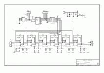
The attenuator is at output of the amp (same as original Pass Labs setup). I am using a Dantimax RelVol3, which is a balanced version of the RelVol1 (I could also have used 2 RelVol1 boards). The RelVol3 schematic is nearly identical to the RelVol1 schematic that is published on the Dantimax website (see below).
Note: I am using different values for the resistors than in this schematic in order to make a 1k attenuator.
R27 and R28 are the load resistors (I have installed 1k RN55D resistors). If you mean "are the outputs (pins 1 of JP3 and JP4) unconnected at any time", the answer is no, the load resistors are always present.
If you mean "are the inputs (pins 1 of JP1 and JP2) unconnected at any time", the situation is less clear to me because I have no idea how the software does the actual switching (in which order are the relays opened or closed when multiple relays need to be changed for a single step, timing, etc.). Could a high value resistor between pins 1 and 2 of JP1 (and JP2) have an effect?
Your help is appreciated

Thanks,
Albert
Attachments
Hi Bfpca,
Thanks for your help. The noise you hear is the clicking of the relays. I tested the RelVol3 board with a 1KHz square wave generator connected to the input of the RelVol3 board and an analog scope connected to the output of the RelVol3 board. The P1.7 amp board was not connected (not even powered during this test).
I understand that it will not be the smooth (infinite step) change I see with a pot, but I assume I should see a clean jump from 1 level to the next, without the distortion.
I built a 23 step 25k shunt attenuator using a mechanical switch for my B1. When I turn the volume up or down in the B1 the sound gets louder or softer but does not distort. I will remove the attenuator from the B1 and try the same test with a 1KHz square wave and scope.
I am unsure what you mean by "leaves the amp inputs open circuit during the switching period of the relays".
The attenuator is at output of the amp (same as original Pass Labs setup). I am using a Dantimax RelVol3, which is a balanced version of the RelVol1 (I could also have used 2 RelVol1 boards). The RelVol3 schematic is nearly identical to the RelVol1 schematic that is published on the Dantimax website (see below).
Note: I am using different values for the resistors than in this schematic in order to make a 1k attenuator.
R27 and R28 are the load resistors (I have installed 1k RN55D resistors). If you mean "are the outputs (pins 1 of JP3 and JP4) unconnected at any time", the answer is no, the load resistors are always present.
If you mean "are the inputs (pins 1 of JP1 and JP2) unconnected at any time", the situation is less clear to me because I have no idea how the software does the actual switching (in which order are the relays opened or closed when multiple relays need to be changed for a single step, timing, etc.). Could a high value resistor between pins 1 and 2 of JP1 (and JP2) have an effect?
Your help is appreciated
Thanks,
Albert
Arghhhh! This is hard to do remotely. I enjoy helping others sort out this sort of problem but it's not easy from a distance. I had a brief look at the schematic but didn't have time to really study it. One thing that I find odd is the inductor L1 that seems to be going from the control circuit power supply ground to the analog ground. Not sure why that is there or if it could be causing a problem.
Have you tried shorting the attenuator inputs so that you have no ac or dc signal on the inputs and then checking to see if you still get the noise on the scope?
Brian
Hi Bfpca,
Thanks for your help, I appreciate it. I emailed Mikkel from Dantimax again but still no reply.
I took the L1 inductor out soon after I first heard the distortion problems (i.e. agnd and gnd no longer connected on relvol3 board). Control 5v psu is completely separate from 60v p1.7 psu, so connection should not be required.
I will try your suggestion and see what happens when I short the inputs. To be continued.
Albert
PS The square wave was generated by a portable (battery powered, so not grounded) dso nano digital scope.
I also tried a 1vpp sine from an owon digital signal generator (mains powered, same powerboard ground as scope) and also saw the distortion.
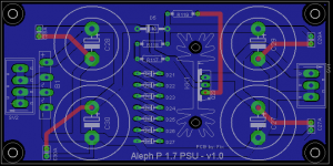
Here are the first preview of the main and psu pcb's.
Main pcb is close as possible to R Stens version.
PSU is based on a version I found on the net.
If there are some interest I can arrange a GB for professional PCB's at low cost as possible.
Main pcb is close as possible to R Stens version.
PSU is based on a version I found on the net.
If there are some interest I can arrange a GB for professional PCB's at low cost as possible.
Attachments
Last edited by a moderator:
Hi Fix,
Boards are looking good!
I have no experience designing boards, so this may be a stupid question.
PWRGND is connected to - terminals of C26 and C25 through a wide red trace. Where is that trace connected to the ground plane on the other side? Or is the PWRGND pad connected to both ground plane and red trace?
What have you designed to be used as heat sink for Q15-Q21? Do you have a specific part in mind? If so, could you mention part#?
Looking at the board, I think you have planned DIP switches for the gain switches. I have heard that jumpers (like those used in computers) are sonically better than DIP switches, but have no idea if that is true or not.
Let me know when you decide to have them made because I think they will be better than the boards I am currently using.
Thanks,
Albert
PS Somewhere in the Aleph threads it is mentioned that ZVP3310A is a good replacement for the IRF9610 in the input stage of the power amps and some say is sounds better. I have no idea if the equivalent part (ZVN3310A) could be used in the P1.7 instead on the IRF610. Perhaps dissipation is too high?
Note that they have different pin assignment than IRF. If a P1.7 using ZVN3310A is feasible, I have no idea if the option to use either ZV or IRF could be incorporated on the board. Perhaps something to look into?
@albertNL
The heat sink is:
Fischer Electronik, SK125/84
SK 125/84 SA - FISCHER ELEKTRONIK - Heat Sink, EU Card, 5.8 °C/W, 28 mm, 84 mm, 84 mm | Farnell element14
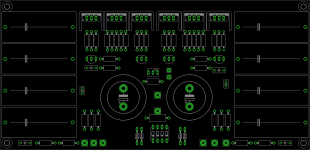
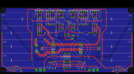
PCB
Red trace is on top.
Blue trace is on bottom.
All grounds are on Bottom side, and also two + traces for the transistors (Can be hard to see on picture) I can send a Hires version if you want.
Dip switch
I did think if I should use relays as Koja's pcb had, but I decided not to since I have other pcbs for audio (Pearl Ono RIAA) were they they use Dipswitches in the Moving Coil circuit without problems, also original version do.
BOM
BOM list is available for easy shopping.
Group buy
I have 3 others that made pre-books. Target price will be ~10 EUR or lower / pcs ( + shipping, customs and vat )
In the next few days I make an Group buy thread, and there we can talk about adding extra features if needed.
The heat sink is:
Fischer Electronik, SK125/84
SK 125/84 SA - FISCHER ELEKTRONIK - Heat Sink, EU Card, 5.8 °C/W, 28 mm, 84 mm, 84 mm | Farnell element14
PCB
Red trace is on top.
Blue trace is on bottom.
All grounds are on Bottom side, and also two + traces for the transistors (Can be hard to see on picture) I can send a Hires version if you want.
Dip switch
I did think if I should use relays as Koja's pcb had, but I decided not to since I have other pcbs for audio (Pearl Ono RIAA) were they they use Dipswitches in the Moving Coil circuit without problems, also original version do.
BOM
BOM list is available for easy shopping.
Group buy
I have 3 others that made pre-books. Target price will be ~10 EUR or lower / pcs ( + shipping, customs and vat )
In the next few days I make an Group buy thread, and there we can talk about adding extra features if needed.
I'd be interested in a set of the boards and probably an extra power supply board...
You also really do not need heat sinks for this. There is no huge amount of heat generated. I built Kojas version last year and used heat sinks. Was a waste of time. Folding the mosfets over and using the ground plane on the PCB's as a heat sink like they did in the original factory version is all you would ever need. And you do have room there to do that with just a little extra layout work.
Mark
Last edited:
Since R Sten is not interested in spreading his design even for Diyers, I will make another layout to keep him happy. I can't see the actual problem since he share it if you ask nicely and are a diyer. But this is his request even for small group buys.
I get back soon as I have another nice layout.
I get back soon as I have another nice layout.
Looks nice !
Small question :
Could you incorporate multiple size of capacitors ?
When i built mine, no holes on the PCB for the caps i wanted to use.
So i had to bridge-wire them.
Regards,
Nick.
Hi Fix,
It is looking good. I have not had time to look at it in detail yet, but Nick's suggestion is good. Not only for the 10uf mkp's but also for the bypass caps.
I have read somewhere that 90 degree angles in the traces are to be avoided, but don't know if there is any truth in it (I have never made a pcb). Perhaps worth checking because some are easy to change/make less "square" without changing the layout.
Thanks!
Albert
Here is first preview of the layout.
Will clean it up much as I can.
Ideas and input are welcome.
Am I correct, that for gain you have included 3 options:
1) fixed resistor,
2) var.resistor and
3) pads for external gain switch or pot.
If so, great idea!
In the original schematic the power supply enters between the 2 large supply caps. While the entry to the left of the left supply cap gives the same electrical connections, I am unsure if the original symmetry had any sonic advantages. The way it was originally drawn, the + and - sections of the amp are completely separate and only meet at the power entry between the supply caps and at the (var.) gain resistor. Would it be worth moving the PSU pads to the center (by moving the gain circuit slightly higher)?
Taking this one step further, I am wondering if there would be any sonic advantage to have 2 separate 3R3 resistors at the power entry, one for each side of the amp, that way separating the + and - sides even more, rather than both sides sharing the same 3R3 resistor, but it is beyond me to answer this question.
There are some discrepancies in hole sizes (e.g. source resistor on right 9610) but I assume this is something to look at when the rest is finalised.
One last thing. I am unsure if I am looking at it correctly or not, but I think there is a trace missing between the drains of the left two (9610 and 610) and right two fets.
I hope to have more time tomorrow.
Albert
@albertNL
Yes, that's one of the extras I'll add soon as I can.
@albertNL
PSU pads, I'm thinking on that, should not do any difference. But might looking better.
I added 3 options for gain stage, as I liked the way R Sten did it.
There some minor minor errors, and I fix that too.
Missing traces near transistors...
@ElectroNick
I don't think that's a problem, but I also like "less square" so it will be fixed.
Will try to have a new preview later today.
Could you incorporate multiple size of capacitors ?
When i built mine, no holes on the PCB for the caps i wanted to use.
So i had to bridge-wire them.
Yes, that's one of the extras I'll add soon as I can.
@albertNL
Am I correct, that for gain you have included 3 options:
1) fixed resistor,
2) var.resistor and
3) pads for external gain switch or pot.
If so, great idea!
In the original schematic the power supply enters between the 2 large supply caps. While the entry to the left of the left supply cap gives the same electrical connections, I am unsure if the original symmetry had any sonic advantages. The way it was originally drawn, the + and - sections of the amp are completely separate and only meet at the power entry between the supply caps and at the (var.) gain resistor. Would it be worth moving the PSU pads to the center (by moving the gain circuit slightly higher)?
Taking this one step further, I am wondering if there would be any sonic advantage to have 2 separate 3R3 resistors at the power entry, one for each side of the amp, that way separating the + and - sides even more, rather than both sides sharing the same 3R3 resistor, but it is beyond me to answer this question. There are some discrepancies in hole sizes (e.g. source resistor on right 9610) but I assume this is something to look at when the rest is finalised. One last thing. I am unsure if I am looking at it correctly or not, but I think there is a trace missing between the drains of the left two (9610 and 610) and right two fets. I hope to have more time tomorrow.
PSU pads, I'm thinking on that, should not do any difference. But might looking better.
I added 3 options for gain stage, as I liked the way R Sten did it.
There some minor minor errors, and I fix that too.
Missing traces near transistors...
@ElectroNick
It is looking good. I have not had time to look at it in detail yet, but Nick's suggestion is good. Not only for the 10uf mkp's but also for the bypass caps.I have read somewhere that 90 degree angles in the traces are to be avoided, but don't know if there is any truth in it (I have never made a pcb).
Perhaps worth checking because some are easy to change/make less "square" without changing the layout.
I don't think that's a problem, but I also like "less square" so it will be fixed.
Will try to have a new preview later today.
And here I'm again 
just started placing everything inside case...
and have question about setting up a gain for P.1.7
the gain should be set via 2Kohm trimer.
the question is, how much gain should I set ?
my system is ;
amareno USB to I2S
I2S input on Najda DSP - I2S output
I2S input on AYA II TDA1541 DAC - SE output
SE input on Aleph P1.7 - BAL output
BAL RelVol3 relay attenuator
(my amplifiers are Aleph X, Aleph mini, IcePower 125ASX2 )
When playing on PC via amareno, AYA II have 2V on output.
I have place 10Kohm resistor on output be twin + and - of balanced output 8which represent load of amplifier)
So, how much gain should I set by triming ?
If I place 10Kohm resistor be twin + and -, how do I get gain ? is gain represent as 2V on input and lets say 3V on BAL output betwin ''+'' and ''0'' = gain of 1.5
Or is gain represnative as 2V on input and voltage betwin ''-'' and ''+''
thanks

O.K.
now I have a problem...
I place two channel into case..all fine
place another two channel and one of them is not working...
on non working I have
around 0.1V over 3.3 for around 59.6v
have 0.61V on R59 and 0V on R44
and 0.63V on R70 and something like 0.1V on R55
what to look for ?
should I try to change Q15 and Q18 ?
Hi Yoke
It looks like you have no current flowing in the left side of the preamp. You should have approx. .6v on R44 and R55 Check to make sure the 10k resistor R 46 is in there correctly on that side and also that Q11 and Q12 are installed correctly. The transistor solder pads are close together so there is also a chance that some of the connections may be shorted.
Let us know what you find.
Brian
- Home
- Amplifiers
- Pass Labs
- Pass Aleph P 1.7 preamp builders thread