Re: Re: Re: Re: Re: a big enough liabilities
Now hold on there buckeroo.")
I hope you don't think I was saying or implying that we should just stick to objective technical parameters. If that's the impression you got, that's not the one I meant to convey.
What I was saying in an admittedly round about way was that typically the self-professed subjectivists, who typically see themselves at odds with the so-called objectivists, are, when you scrape away the rhetoric, objectivists themselves and what you really have are just two groups of objectivists. The only difference is that one group believes that once the objective parameters are below a certain level it doesn't matter and the other group does not.
Personally, I no longer obsess over objective parameters. Once I stopped obsessing over objective parameters and only my resopnse to the end result (i.e. the music), I found that I actually preferred some things which I never would have considered doing before and indeed didn't even like when I'd tried them before.
I think obsessing over objective matters tends to lead to something of a self-fulfilling prophecy. God knows there's enough psychology involved in our subjective perceptions.
And I'm not saying there's anything wrong with obsessing over objective issues. Whatever gets your foot tapping is the only "right" approach. I've just found the approach I take now more enjoyable for me.
se
mikek said:Amen!.....Yes lord!!![/B]
Now hold on there buckeroo.
I hope you don't think I was saying or implying that we should just stick to objective technical parameters. If that's the impression you got, that's not the one I meant to convey.
What I was saying in an admittedly round about way was that typically the self-professed subjectivists, who typically see themselves at odds with the so-called objectivists, are, when you scrape away the rhetoric, objectivists themselves and what you really have are just two groups of objectivists. The only difference is that one group believes that once the objective parameters are below a certain level it doesn't matter and the other group does not.
Personally, I no longer obsess over objective parameters. Once I stopped obsessing over objective parameters and only my resopnse to the end result (i.e. the music), I found that I actually preferred some things which I never would have considered doing before and indeed didn't even like when I'd tried them before.
I think obsessing over objective matters tends to lead to something of a self-fulfilling prophecy. God knows there's enough psychology involved in our subjective perceptions.
And I'm not saying there's anything wrong with obsessing over objective issues. Whatever gets your foot tapping is the only "right" approach. I've just found the approach I take now more enjoyable for me.
se
Peter Daniel said:You said it all very nicely. Just for one post like that, it was worth bringing this thread back
Wow. Seeing as I didn't say a word about output stages or slew rates I figured it'd more likely have been tossed back into Off Topic.
Thank you for the kind words.
se
Size matters
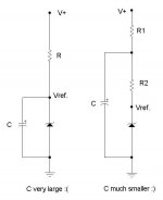
I guess I don't quite get this obsession for small capacitor values. A 1000uF is a reasonably sized cap for an electrolytic. Placing the cap across the zener shunts the zener noise at frequencies where the capacitor impedance becomes less than the zener impedance of and lowers the impedance seen at the voltage reference point. The power supply terminal for several op amps is across this zener in the original context of this discussion. A low AC impedance for the op amp supply is very beneficial. Your circuit on the right for the smaller cap value has neither of these features and I can't see the point of the topology. This is pretty simple circuit that is commonly used.
I guess I don't quite get this obsession for small capacitor values. A 1000uF is a reasonably sized cap for an electrolytic. Placing the cap across the zener shunts the zener noise at frequencies where the capacitor impedance becomes less than the zener impedance of and lowers the impedance seen at the voltage reference point. The power supply terminal for several op amps is across this zener in the original context of this discussion. A low AC impedance for the op amp supply is very beneficial. Your circuit on the right for the smaller cap value has neither of these features and I can't see the point of the topology. This is pretty simple circuit that is commonly used.
Attachments
Once again
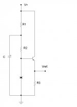
Thie circuit below is flawed for the same reasons as the previous one.A better way to do it is by biasing the zener from the V+ supply with resistor and filtering the zener noise (and the attenuated V+ noise across the zener) with an RC circuit after the zener is the usual approach. The base of the transistor would be connected to the junction of the capacitor and the resistor to the zener. This will filter the noise and reduce the effective impedance of the node by Hfe of the transistor. (until the impedance at the junction the resistor from the zener and the capacitor to ground drops below a few 10s of ohms) At high frequencies the capacitor actually has much less impedance than the emitter of the transistor. Another capacitor to ground at the emitter is often used for this reason. This are extremely common circuits and I have seen this capacitor bypassed emitter follower supply in many audio supplies. These are even commonly used as regulators for vacuum tube circuits.
Thie circuit below is flawed for the same reasons as the previous one.A better way to do it is by biasing the zener from the V+ supply with resistor and filtering the zener noise (and the attenuated V+ noise across the zener) with an RC circuit after the zener is the usual approach. The base of the transistor would be connected to the junction of the capacitor and the resistor to the zener. This will filter the noise and reduce the effective impedance of the node by Hfe of the transistor. (until the impedance at the junction the resistor from the zener and the capacitor to ground drops below a few 10s of ohms) At high frequencies the capacitor actually has much less impedance than the emitter of the transistor. Another capacitor to ground at the emitter is often used for this reason. This are extremely common circuits and I have seen this capacitor bypassed emitter follower supply in many audio supplies. These are even commonly used as regulators for vacuum tube circuits.
Attachments
Fred Dieckmann said:I guess I don't quite get this obsession for small capacitor values. A 1000uF is a reasonably sized cap for an electrolytic. Placing the cap across the zener shunts the zener noise at frequencies where the capacitor impedance becomes less than the zener impedance of and lowers the impedance seen at the voltage reference point. The power supply terminal for several op amps is across this zener in the original context of this discussion. A low AC impedance for the op amp supply is very beneficial. Your circuit on the right for the smaller cap value has neither of these features and I can't see the point of the topology. This is pretty simple circuit that is commonly used.
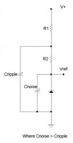
Ahhh.....i take it you now accept that placing a capacitor across a power supply zener reference with a view to lowering its output resistance, or reducing power supply rail ripple simply won't work, and is very inefficient of cap. size respectively......
...On the the subject of zener noise, .....yes....a great many published circuits, including current-source references, place a cap. across the zener with a view to filtering noise....
This is indeed a good idea, as one can expect sufficient attenuation in the audio mid-band, where the ear is most sensitive to such.......one solution is given in attached figure...
For a typical zener impedance of 20 ohms at room temp, and 10mA, 470u should work well....
Also see chapter 10 of the following:
www.onsemi.com/pub/Collateral/DL150-D.PDF
Fred Dieckmann said:Thie circuit below is flawed for the same reasons as the previous one.A better way to do it is by biasing the zener from the V+ supply with resistor and filtering the zener noise (and the attenuated V+ noise across the zener) with an RC circuit after the zener is the usual approach. The base of the transistor would be connected to the junction of the capacitor and the resistor to the zener. This will filter the noise and reduce the effective impedance of the node by Hfe of the transistor. (until the impedance at the junction the resistor from the zener and the capacitor to ground drops below a few 10s of ohms) At high frequencies the capacitor actually has much less impedance than the emitter of the transistor. Another capacitor to ground at the emitter is often used for this reason. This are extremely common circuits and I have seen this capacitor bypassed emitter follower supply in many audio supplies. These are even commonly used as regulators for vacuum tube circuits.
do you mind posting the circuit?
It has to be said that the emitter follower would have to run at fairly high quiescent current in order to effect a significant reduction in the zeners impedance.....
Attachments
The zener diode is particularly noisy at higher voltages. The quietest zener is 5.6 volts; at this voltage noise is very low indeed. Perhaps a better option is to make a variable zener, using an NPN transistor with a 5.6V zener in its emitter, and a resistive divider between collector, base and the bottom of the zener.
By fixing the lower resistor in this string (R1), base to anode of zener, and setting a value of the base to collector resistor (R2) far above this a la Vbe multiplier, you can fashion a very effective and quiet Zener.
The total voltage from anode (bottom) of zener and collector (top) of this configuration is given by Vt = (6.2(1 + R2/R1). For R1 of 1K, and R3 of 3K3, the total voltage of this composite zener is 26.66 volts. The only caveats are that the current through the voltage divider should be at least 15 times the base current of the transistor and at least five times lower than the collector current; and that the zener should be run at no more than 30% its commercial continuous rating. This ensures good temperature compensation, low noise, and tolerance of varying betas.
Cheers,
Hugh
AKSA said:The zener diode is particularly noisy at higher voltages. The quietest zener is 5.6 volts; at this voltage noise is very low indeed. Perhaps a better option is to make a variable zener, using an NPN transistor with a 5.6V zener in its emitter, and a resistive divider between collector, base and the bottom of the zener.
By fixing the lower resistor in this string (R1), base to anode of zener, and setting a value of the base to collector resistor (R2) far above this a la Vbe multiplier, you can fashion a very effective and quiet Zener.
The total voltage from anode (bottom) of zener and collector (top) of this configuration is given by Vt = (6.2(1 + R2/R1). For R1 of 1K, and R3 of 3K3, the total voltage of this composite zener is 26.66 volts. The only caveats are that the current through the voltage divider should be at least 15 times the base current of the transistor and at least five times lower than the collector current; and that the zener should be run at no more than 30% its commercial continuous rating. This ensures good temperature compensation, low noise, and tolerance of varying betas.
Cheers,
Hugh
...good idea....
...Hugh...have you considered using two-pole compensation in your designs?
Re: Re: ....Interesting....
...to zip or not to zip...that is the question...
Steve Eddy said:
Why are you ZIPping up GIFs? I spent far more time firing up WinZip and unZIPping it than that 1% compression saved me in downloading it.
se
...to zip or not to zip...that is the question...
Hi Mikek,
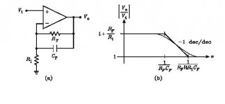
In fact, no, I do not use two pole compensation at this stage. Without a lot of experimentation as to its advantages, I have almost persuaded myself it is problematic. As I understand it, two pole compensation is a second order lag compensation network around the voltage amplifier, from collector to base. This enables a higher frequency to be set in this stage, since the slope is 6dB higher at 12dB/octave, and the theory goes that a higher pole frequency will improve the sonics because the caps can be reduced in (effective) size.
However, there appear to be issues here. I have not yet seen a two pole scheme where the lesser of the two caps, the upper one, is actually less than the single cap which would be used in single pole compensation. Typically the values chosen are 100pF and 1nF, where a single pole regime would use 100pF. I would say that unless the upper cap can be reduced to maybe 47pF, there is little to justify the increased complexity, particularly as the quality of these caps is important to the sonics and a quality 1nF cap is actually more expensive than a 100pF!
There are other considerations. If the amplifier is made with very fast semiconductors, then the phase shift will be less since group delay is reduced. This will also force up the pole, the point at which negative global feedback turns positive - and causes oscillation. Thus the compensation network need only act at this higher frequency, very much outside the ambit of the audible range. The most significant semiconductor in this instance is, of course, the voltage amplifier stage, which is in common emitter. Thus a 100MHz or higher rating on this pivotal device is mandatory.
Lastly, one must consider real world loads, which are inevitably reactive. The typical scenario seems to be high capacitance, particularly with electrostatics, and some means of shifting the phase to correct this in advance might be in order. Phase compensation, a small cap used between the voltage amplifier output and the feedback node, is a very useful method of improving tolerance to highly capacitive loads, and my amplifier designs use both lag and phase compensation. This method is highly favoured by Linsley Hood, a worthy guru. I find this approach difficult to get right, but very effective for stability, and much simpler than two pole lag compensation.
Cheers,
Hugh
No I am really confused.
No, I don't, quite the contrary. The whole point of this discussion was that the simple shunt zener regulator in the amp under discussion, would benefit from a larger capacitor across it to lower the noise, lower the supply impedance seen by the op amps, and could be done with a reasonable sized cap with a corner frequency below 20Hz. I didn't think it would be a controversial topic. As for follower topologies, RC fitering of the zener noise before the base connection of the follower is the most sensible topology for reduction of zener noise and increasing the PSRR. I see that 470 uF is an "efficient cap size" but I take it that 1000uF isn't. Perhaps you could weigh in on 680uF...........
mikek said:
Ahhh.....i take it you now accept that placing a capacitor across a power supply zener reference with a view to lowering its output resistance, or reducing power supply rail ripple simply won't work, and is very inefficient of cap. size respectively......
For a typical zener impedance of 20 ohms at room temp, and 10mA, 470u should work well....
.....
No, I don't, quite the contrary. The whole point of this discussion was that the simple shunt zener regulator in the amp under discussion, would benefit from a larger capacitor across it to lower the noise, lower the supply impedance seen by the op amps, and could be done with a reasonable sized cap with a corner frequency below 20Hz. I didn't think it would be a controversial topic. As for follower topologies, RC fitering of the zener noise before the base connection of the follower is the most sensible topology for reduction of zener noise and increasing the PSRR. I see that 470 uF is an "efficient cap size" but I take it that 1000uF isn't. Perhaps you could weigh in on 680uF...........
AKSA said:Hi Mikek,
However, there appear to be issues here. I have not yet seen a two pole scheme where the lesser of the two caps, the upper one, is actually less than the single cap which would be used in single pole compensation. Typically the values chosen are 100pF and 1nF, where a single pole regime would use 100pF. I would say that unless the upper cap can be reduced to maybe 47pF, there is little to justify the increased complexity, particularly as the quality of these caps is important to the sonics and a quality 1nF cap is actually more expensive than a 100pF!
Hi Hugh
I think you'll find that the component values for most published designs using two-pole compensation, including self's, are incorrect.....there is simply no need for a 1nF......see post #41..
if for instance, you've decided on 100pF as your miller compesation capacitor, Ccomp., then select C1=150pF, and C2=300pF, so that Ccomp=C1//C2. Then chose R to set the location of your zero.....ergo the frequency at which open-loop roll-off reverts to a single pole regime.....using:
Fz=1/{2*pi*(C1//C2)R}
...1K works well....
this should reduce the current demand on your input stage at !kHz at least 20 fold.......!
this is especially important for designs that eschew a first stage current mirror.
AKSA said:
Phase compensation, a small cap used between the voltage amplifier output and the feedback node, is a very useful method of improving tolerance to highly capacitive loads, and my amplifier designs use both lag and phase compensation. This method is highly favoured by Linsley Hood, a worthy guru. I find this approach difficult to get right, but very effective for stability, and much simpler than two pole lag compensation.
Cheers,
Hugh
The Linsley-Hood scheme is merely the conversion of the gain stage into a low pass shelving amplifier, with the output stage excluded....see...figure 1.32 in....:
http://users.ece.gatech.edu/~mleach/ece4435/chap01.pdf
Excluding the output stage thus...is sub-optimal, as this occurs at frequencies where output stage distortion is at its worst....
Attachments
AKSA said:Ah, Mikek,
sub-optimal it may be, but it confers excellence performance into capacitive loads and assists with real world stability!
Ultimately, this sounds better. Who am I to reject it out of hand?
Cheers,
Hugh
'...assists with real world stability...'
...i am not entirely certain that this is true....
Mikek,
No problem!! I know it's true!
Cheers,
Hugh
...i am not entirely certain that this is true....
No problem!! I know it's true!
Cheers,
Hugh
Whom to believe?
I think I will take the word of some who actually designs and sells a highly regarded amplifier over someone likes to quote technical articles without the experience of actually building and measuring amplifiers. It may come as a shock..... but stability into widely varying load impedances is much more important than high slew rate or bandwidth far exceeding the audio range. Most of the good amps I have heard have closed loop bandwidths in the 100 kHz to 200 kHz region and conservative phase margins. I guess it is a lot easier to read about something than to actually go do it though. Arrogance and ignorance are two traits that don't go together very well in my experience.
I think I will take the word of some who actually designs and sells a highly regarded amplifier over someone likes to quote technical articles without the experience of actually building and measuring amplifiers. It may come as a shock..... but stability into widely varying load impedances is much more important than high slew rate or bandwidth far exceeding the audio range. Most of the good amps I have heard have closed loop bandwidths in the 100 kHz to 200 kHz region and conservative phase margins. I guess it is a lot easier to read about something than to actually go do it though. Arrogance and ignorance are two traits that don't go together very well in my experience.
Whom to believe?
I choose Phred and Hugh.
In my understanding another reason to avoid high slew rate output stages is that this is another means of exciting power supply resonances.
High PSRR or low PSRR, these effects are audible.
Some amplifiers that I have heard such as Metaxas amplifiers with published very high slew rates and bandwidths on first impression sound very 'fast', but after about 5 minutes drive me out of the room as fast as I can go.
In addition these amplifiers (earlier models) are very fragile and go SPLATT at the merest provocation.
In my view slew rates faster than reasonably necessary are not required, and can be seriously deleterious.
Load stability is of the utmost importance in my books, and cannot be substituted.
Eric.
I have to concur with Eric and Fred.
Load stability is paramount, since failure to ensure it results inevitably in a blown amplifier, with possible destruction of the speakers as well - tweets through HF oscillation, and woofs through overcurrent.
The world is littered with examples of wonderful sounding amplifiers which blew up in the real world. Truth is, one very good reason NOT to use global negative feedback is the difficulty such amps have with real world loads, and there is hardly a speaker system on the planet which does not present highly reactive loading.
One of the comic ironies of the electrostatic speaker is that the only feedback amplifiers eminently suited to driving them bear more resemblance to welding machines than elegant devices for amplifying recorded music. I've always felt that it is a great tragedy that those beautiful ESL63s are most reliably driven from a power take off via a Lincoln arc welding generator!
Of course, if you go tube, the story is different.
However, is there a non-global feedback SS output stage which can cope with highly reactive loads? You betcha! A single ended mosfet!!
Cheers,
Hugh
AKSA said:However, is there a non-global feedback SS output stage which can cope with highly reactive loads? You betcha! A single ended mosfet!!
So when can we expect to see one in your product lineup?
se
- Status
- This old topic is closed. If you want to reopen this topic, contact a moderator using the "Report Post" button.
- Home
- Amplifiers
- Solid State
- Output stages with gain Enhance Slew rate