Should I use a single electrolytic?
Jim,
Jocko,
Thanks for your info.
If use separate large reservoir electrolytics for each IC these will be connected in parallel across the common digital line. This could give rise to resonance.
Should I use a single electrolytic?
Note:
Elso kwak uses 0.1uF ceramic across each IC in his reclocker. The ICs have ferrites in the supply lines. Finally a single electrolytic capacitor serves as a reservoir for entire reclocker circuit. I wonder if this was a deliberate decision to avoid parallel connection of multiple reservior electrolytics- thus avoid resonance- or was this simply cost reduction?
jean-paul said:
Just curious, did you use BG only as well ( without the triple bypass) ? Bypassing BG did not bring much here, it became worse when bypassed with ceramic caps....
In fact I stopped bypassing some time ago as I like one good cap better when implemented well. I am talking soundwise this time, not technically/measurements. I even rediscovered using plain BCcomponents electrolytics and I like them.
Electrolytics have made great progress in the last years and although my prejudice against them is hard to get rid off I am starting to judge them right. How difficult it can be to readjust to something one got used to. In the eighties I bypassed every cap I saw and now I am using just one....
Same thing with BG N series. Put 4.7 uF MKT in my preamp to discover ( again ! ) that BG N was better despite being an electrolytic.
I just checked ceramic bypassing yesterday, and here's what I think about it:
http://www.diyaudio.com/forums/showthread.php?s=&postid=358034#post358034
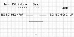
How about this decoupling scheme?
How about this decoupling scheme?
The key features:
1) No capacitors directly connected in parallel. There is resistive damping between each capacitor. (This should reduce possibility of resonance within the arrangement and across the board)
2) Use of inductor and ferrite to filter a wide range of rf
3) Small bypass capacitor with short PCB trace near IC
4) Larger reservior capacitor
5) Low noise, quality capacitors throughout
Anyone tried something similar?
(P.S. looks a little like TNT Convertus PSU arrangement)
Attachments
Petter said:I read the thread but was not quite sure what you thought about ceramic bypassing once finished reading.
I think ceramic bypassing spice up the sound a bit. In my case it worked for better. Without bypasses the sound seemed to be a bit dry and not involving enough ( although very proper). It wasn't bad, but for my taste, not alive enough and slightly boring.
I remembered how this DAC can sound and I was missing it. After addiong ceramic pairs, I achieved more liquidity and more envolvement. Slightly more 3 dimentionality as well. Initially, it seemed a bit more brighter, but considering other added virtues, I think its the price worth paying.
What I suggest, don't desregard those caps and try for yourself, it might be your cup of tea
")
Re: How about this decoupling scheme?
I'm not sure if you read my link, so here I quote it:
"As a matter of fact, I just completely changing out the bypass
structure of the CS8412 and SM5842AP (having recently replaced the
DF1700) to match that of the bypass on the analog side, which worked
so well. The results were amazing and not expected. I had initially
bypassed these parts with a 3.3uF tantalum in parallel with an AVX
1210 220nF X7R chip cap and replaced the 10uF 'lytic at the output of
the 7805 with a 10uF tantalum, apparently this combination was better
than stock but not as good as the latest improvement.
The best combination I have found to date that works by calculation,
simulation, measurement, and listening is as follows:
A Panasonic HFQ 'lytic, 120uF/25V paralleled with an AVX 0612
270nF/25V Z5U chip cap paralleled with an AVX 0612 10nF/50V X7R chip
cap. Note that these chip caps are 0612s, not 1206s. This yields a
nearly perfectly resitive driving point Z out to about 90MHz or so.
The residual inductance is on the order of 180pH which is swamped by
the internal parasitics of the bypassed device's leadframe and bond
wires. The 10nF should be mounted to the board first with the 270nF
on top so that inductance at high frequencies is minimized. This is a
very tedious task (having installed 28 sets of these on the DAC-1 I
can swear by that) but it can be done and provides a serious
improvement in performance by itself.
The rest of the bypass structure is defined by the regulator type
feeding the rail. If it is a 7805 or 7905 reg, then bypass it at its
output with a Panasonic HFQ 'lytic, 12000uF/6.3V...if it is a 7815 or
7915, use an HFQ 6800uF/25V 'lytic. These will closely cancel the
apparent inductive output impedance of the regs and provide a nearly
resitive driving point Z at the source of power feed network. Do not
use FA type capacitors as their ESR is too low to provide the correct
damping. Keep all the leads short and it should work just fine in any
other application. As a final measure, use Panasonic FA series caps
as the main filter caps as that is where their very low ESR matters
the most by minimizing ripple voltage due to the ripple current from
the rectified secondary voltage of the transformer...this matters
whether the filter topology is a choke input or a capacitor input
type.
Hope this helps,
Pete
P.S.: And if you ever see this type of bypass in a future
product...remember you saw it here it first...;-)
"
Oli said:
Anyone tried something similar?
I'm not sure if you read my link, so here I quote it:
"As a matter of fact, I just completely changing out the bypass
structure of the CS8412 and SM5842AP (having recently replaced the
DF1700) to match that of the bypass on the analog side, which worked
so well. The results were amazing and not expected. I had initially
bypassed these parts with a 3.3uF tantalum in parallel with an AVX
1210 220nF X7R chip cap and replaced the 10uF 'lytic at the output of
the 7805 with a 10uF tantalum, apparently this combination was better
than stock but not as good as the latest improvement.
The best combination I have found to date that works by calculation,
simulation, measurement, and listening is as follows:
A Panasonic HFQ 'lytic, 120uF/25V paralleled with an AVX 0612
270nF/25V Z5U chip cap paralleled with an AVX 0612 10nF/50V X7R chip
cap. Note that these chip caps are 0612s, not 1206s. This yields a
nearly perfectly resitive driving point Z out to about 90MHz or so.
The residual inductance is on the order of 180pH which is swamped by
the internal parasitics of the bypassed device's leadframe and bond
wires. The 10nF should be mounted to the board first with the 270nF
on top so that inductance at high frequencies is minimized. This is a
very tedious task (having installed 28 sets of these on the DAC-1 I
can swear by that) but it can be done and provides a serious
improvement in performance by itself.
The rest of the bypass structure is defined by the regulator type
feeding the rail. If it is a 7805 or 7905 reg, then bypass it at its
output with a Panasonic HFQ 'lytic, 12000uF/6.3V...if it is a 7815 or
7915, use an HFQ 6800uF/25V 'lytic. These will closely cancel the
apparent inductive output impedance of the regs and provide a nearly
resitive driving point Z at the source of power feed network. Do not
use FA type capacitors as their ESR is too low to provide the correct
damping. Keep all the leads short and it should work just fine in any
other application. As a final measure, use Panasonic FA series caps
as the main filter caps as that is where their very low ESR matters
the most by minimizing ripple voltage due to the ripple current from
the rectified secondary voltage of the transformer...this matters
whether the filter topology is a choke input or a capacitor input
type.
Hope this helps,
Pete
P.S.: And if you ever see this type of bypass in a future
product...remember you saw it here it first...;-)
"
Don't forget the key to making all this work:
Keep the loop small to minimise EMI.
I believe that Guido Tent demonstrates this in the link that he refers to. Required reading.
(Hope the url is in this thread somewhere, 'cuz I am not certain what it is.)
Ferrites don't really "filter" RF they absorb it. Their resistance at high frequencies keeps parasitic resonances down, without creating IR losses at DC like a resistor would.
Oli:
Small caps are used close in as they become self-resonant at a frequency hopefully higher than what is present. Too low, and they will become self-resosnant at a point below the operating frequency.
Check Wima's site.......they should show how SRF is a function of capacitance for various values. (At least if their site is like their catalog.) This may give you further insight as to how all this works.
Jocko.
Hi,
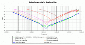
there is no point in stacking various ceramic capacitors. Above resonance impedance is governed by parasitic inductance which is the same for all same size capacitors. Only effect of stacking is reducing inductance by paralleling chips. But you could use same value chips for that, in fact higher capacitance will give better overall results. The only means of improving decoupling efectiveness is reducing parasitic inductance. The only way of reducing parasitic inductance is keeping LOOP AREA small and NOT using short tracks spaced 5mm apart. Also using capacitors with small intrinsic inductance helps. Of course there is no point of using DIP chips instead of SMDs, if they are abailable.
New types of low inductance capacitors are from AVX and from X2Y.
Attached is picture showing effectiveness of stack of 5 various caps (green) against one X2Y cap (blue).
Best regards,
Jaka Racman
Attachments
Jocko Homo said:
I believe that Guido Tent demonstrates this in the link that he refers to. Required reading.
(Hope the url is in this thread somewhere, 'cuz I am not certain what it is.)Jocko.
it is here
http://www.tentlabs.com/Info/Articles/Supply_decoupling.pdf
cheers
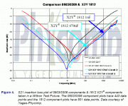
You plots reinforce what I suspected...
Jaka,
You plots reinforce what I suspected...
- A smaller value of capacitor will have a higher resonant frequency.
- A larger value of capacitor will have a lower resonant frequency.
- The larger capacitor has lower e.s.r. and has greater attenuation than the smaller capacitor throughout the range.
So what if we used a large capacitance, low esr electrolytic- e.g. 50uF?
This should be fine for decoupling as long as traces were kept short. In addition it would act as an energy reservior. Since there are no parallel capacitors there would be less chance of oscillation.
The enemy is lead inductance- Historically ceramics were developed as a cost effective and compact capacitor for use in early computers. They facilitate shorter traces- that's the only reason why they're good. As Guido states in his article (see Guido's link) Compared with older electrolytics - "Modern electrolytics are far better Rf performers."
Keep the loop tight!
You guys might want to check out the semiconductor capacitors http://www.vishay.com/capacitors/silicon/ which might be interesting for decoupling.
My other research indicates that the caps recommended by Peter Daniel from AVX appear very smartly executed - the 0612's X7R is available up to 1uF/10V which is getting kind of radical. It is getting increasingly likely that I will use only a single AVX for digital decoupling - 0306 .22uF 10V looks like a great candiate since it should be possible to fit it incredibly close to pins and it takes up minimal board area. My guess is that Peter Daniel might even consider mounting this unit vertically at .61 by .81mm total board space ...
Petter
Anyone tried OsCon and BGs in the same supply line?
Anyone tried OsCon and BGs in the same supply line?
We're not talking about decoupling here; rather the elimition of residual supply noise-
- Initally use Os-con to clean up
- In addition use BG to reduce the noise floor even lower
Anyone tried OsCon and BGs in the same supply line?
We're not talking about decoupling here; rather the elimition of residual supply noise-
- Initally use Os-con to clean up
- In addition use BG to reduce the noise floor even lower
Jaka Racman said:Hi,
seems that there are better alternatives than 0306.
Jaka Racman
That would be great but for one or two glitches.
1. The X2Y chips require more complex routing
2. The X2Y technology chips appear difficult to purchase - where can one get them?
3. The size of the 1812 chips means adding "significant" trace lenght when using really small digital devices.
4. Silicon chips posted earlier provide even better high frequency performance as far as I can eyeball it.
Naturally, I welcome any good alternatives, but for me the AVX chips will likely be "optimal".
Petter
1. The X2Y chips require more complex routing
2. The X2Y technology chips appear difficult to purchase - where can one get them?
3. The size of the 1812 chips means adding "significant" trace lenght when using really small digital devices.
4. Silicon chips posted earlier provide even better high frequency performance as far as I can eyeball it.
1. Depends on the application, sometimes they are even more suitable.
2. Farnell carries them.
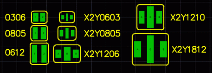
3. 0306 recommended footprint is not small either. Also X2Ychips come in smaller sizes. Below is a picture of recommended footprints for both types. I do not think that 1812 is optimum solution either, but smaller sizes still outperform similarly sized high aspect caps. But you can not solder them directly on the component leads.
4. Fres=2.21GHz, C=12pF => L=432pH, not better than 0306. Eyeballing can be deceptive.
Best regards,
Jaka Racman
Attachments
Surely all this talk about low inductance SMD devices is rather academic.
Surely all this talk about low inductance SMD devices is rather academic.
The PCB trace between the power pins will dominate the inductance and impose the most severe frequency limitations. The quoted theoretical GHz limits are impossible in practice! Clearly SMD decoupling capacitors do reduce the loop length, but we could obtain similar gains by using SMD chips in the first place- or better still use SMD chips and capacitors.
0.1uF caps have become a fashionable 'rule-of-thumb' to improve noise. I believe that the ideal decoupling capacitor will have the highest value in the smallest package, to allow shortest traces.
My point- SMD is good, but only because it enables short traces. The inductance of a non-SMD device imposes less of a limitation on system performance- trace length is the enemy. The only signifianct way forward is to go for full SMD and to shorten the loop.
Back to the main thread...
I have had another thought.... this time concerning ferrites...
Ferrites are advocated in the supply lines of digital ICs
Are ferrites a good idea for the ground returns to the power supplies?
Note: I am not talking about separating grounds between individual ICs with inductors - this would spell disaster.
- Status
- This old topic is closed. If you want to reopen this topic, contact a moderator using the "Report Post" button.
- Home
- Source & Line
- Digital Source
- Optimum Decoupling of Digital ICs