There may come some noises over the clock signal or on the transmission line when you touch the wires, which it alter signal level/quality, so the multichannel DAC it loose the clock (on/off...). .
Thanks Coris, your experience and mine leads us to think similarly.
Cheers, Joe
More than just a thought experiment....
PART ONE
CHALLENGE: IMPROVE NEXT GENERATION OPPO AT NEAR ZERO ADDED COST:
Three areas that Oppo can strengthen the audio performance while adhering to their current manufacturing methods. We shall use the existing model Oppo BDP-105 as a starting point.
This will prove to be more than just a thought experiment, as we have an actual working sample.
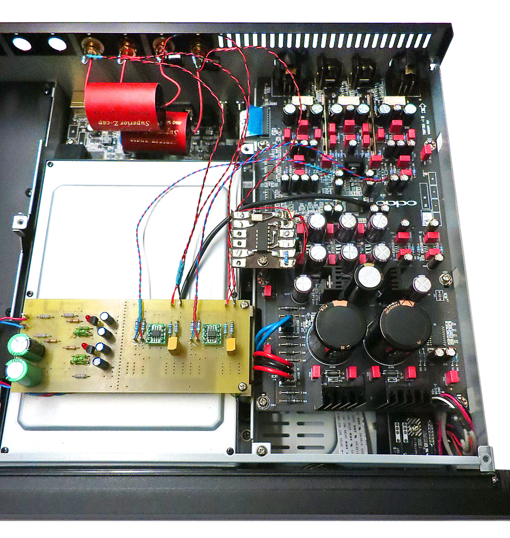
(Please note above: We have dispensed with the Multi-Channel Board - the Oppo 105 works quite well in Stereo only mode without that larger PCB. The holes that are used for RCA outputs are now the new outputs via new RCA sockets. I have two sets to choose from, one pair is using 100uF Silmic output caps [Oppo's choice] and genuine audiophile grade 3.3uF Jantzen Superior Reds.)
We know from John Curl that the guys at Oppo are clever engineers, but they have little experience with high-end. They have turned to others to design the post-DAC circuit, for the unbalanced outputs (which are our primary concern here), the balanced (we can look closely at that later) and finally the headphone circuit.
What they have achieved with the current model is credible at the price point the Oppo 105 is at now. But we want them to do even better and get them to wipe the floor with the competition? This alone should motivate Oppo to consider the alternative presented here.
So the purpose of this exercise is: What can we do to make the next Oppo 115(?) a real high-end performer in the proper sense of the word and make it perform on a level that would be completely beyond the ordinary, but at little or indeed zero cost added.
There are three areas that needs to be strengthened:
1. The post-DAC circuit. This one is the obvious one to tackle and is also the main challenge. We must take it beyond the usual opamp performance - and since opamps are so convenient for something at this price point, it was apparent that a different and yet similar device could be employed in a non-opamp mode. It must be the same SOIC form factor as the existing LM4562, so that rules out a raft of devices.
The OPA-660 is no longer available and that would have been my first choice, and the AD844 form factor is wrong (why 16 pin, and also expensive). The one that should be tried is the OPA-860. Certainly not the perfect choice. That would have been the OPA-660, where output Buffer was not an opamp, but discontinued. But its replacement is OPA-860, and looking at the specs, the opamp buffer is current feedback (and does not have 90 degree phase shift that usual voltage feedback opamps have. I consider that an advantage.
So what will be presented below will be based on the OPA-860.
2. The Clocking. Here we will propose using a single 54MHZ SAW oscillator to feed the Sabre DACs. A divide-by-two chip will get you the 27MHZ required by the Mediatek DSP chip, the Master Clock.
3. Power Supply. The suggestion is a rather modest one - no overhauling or major component replacement regime (good for those who basically are selling you parts and that alone rules it out on cost grounds). Here I will name a single component that can be used on both the Sabre DAC, the SAW oscillator and also by-pass capacitors for the OPA-860 power supply pins. On the Sabre DAC it reduces the noise floor and the same component also works a treat for those other tasks - and keeps inventory simple.
Next: Part Two
.
PART ONE
CHALLENGE: IMPROVE NEXT GENERATION OPPO AT NEAR ZERO ADDED COST:
Three areas that Oppo can strengthen the audio performance while adhering to their current manufacturing methods. We shall use the existing model Oppo BDP-105 as a starting point.
This will prove to be more than just a thought experiment, as we have an actual working sample.
(Please note above: We have dispensed with the Multi-Channel Board - the Oppo 105 works quite well in Stereo only mode without that larger PCB. The holes that are used for RCA outputs are now the new outputs via new RCA sockets. I have two sets to choose from, one pair is using 100uF Silmic output caps [Oppo's choice] and genuine audiophile grade 3.3uF Jantzen Superior Reds.)
We know from John Curl that the guys at Oppo are clever engineers, but they have little experience with high-end. They have turned to others to design the post-DAC circuit, for the unbalanced outputs (which are our primary concern here), the balanced (we can look closely at that later) and finally the headphone circuit.
What they have achieved with the current model is credible at the price point the Oppo 105 is at now. But we want them to do even better and get them to wipe the floor with the competition? This alone should motivate Oppo to consider the alternative presented here.
So the purpose of this exercise is: What can we do to make the next Oppo 115(?) a real high-end performer in the proper sense of the word and make it perform on a level that would be completely beyond the ordinary, but at little or indeed zero cost added.
There are three areas that needs to be strengthened:
1. The post-DAC circuit. This one is the obvious one to tackle and is also the main challenge. We must take it beyond the usual opamp performance - and since opamps are so convenient for something at this price point, it was apparent that a different and yet similar device could be employed in a non-opamp mode. It must be the same SOIC form factor as the existing LM4562, so that rules out a raft of devices.
The OPA-660 is no longer available and that would have been my first choice, and the AD844 form factor is wrong (why 16 pin, and also expensive). The one that should be tried is the OPA-860. Certainly not the perfect choice. That would have been the OPA-660, where output Buffer was not an opamp, but discontinued. But its replacement is OPA-860, and looking at the specs, the opamp buffer is current feedback (and does not have 90 degree phase shift that usual voltage feedback opamps have. I consider that an advantage.
So what will be presented below will be based on the OPA-860.
2. The Clocking. Here we will propose using a single 54MHZ SAW oscillator to feed the Sabre DACs. A divide-by-two chip will get you the 27MHZ required by the Mediatek DSP chip, the Master Clock.
3. Power Supply. The suggestion is a rather modest one - no overhauling or major component replacement regime (good for those who basically are selling you parts and that alone rules it out on cost grounds). Here I will name a single component that can be used on both the Sabre DAC, the SAW oscillator and also by-pass capacitors for the OPA-860 power supply pins. On the Sabre DAC it reduces the noise floor and the same component also works a treat for those other tasks - and keeps inventory simple.
Next: Part Two
.
Last edited:
PART TWO
POST-DAC CIRCUIT:
Clearly a lot of work was done here - and in the last two weeks a number of things had to be sorted and as you would expect, while I had certain ideas in mind, there would be issues that would arise that would need to be addressed.
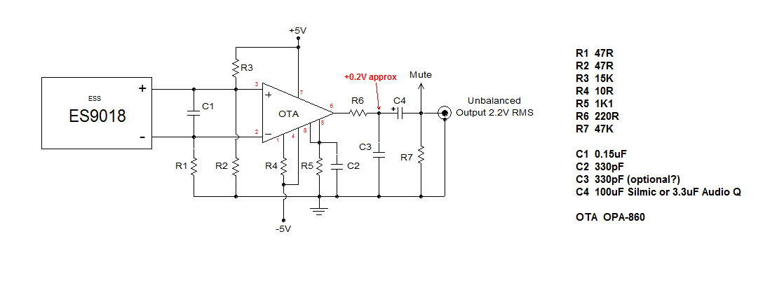
DC Stability: One thing is that opamps have an inherit 'servo' action that means that open-loop DC parameters that can vary from one component or batches - that the DC on the output will be easy to get to near zero mVolt. As we don't use feedback, I found that certain values simply did not work as I was getting to great sample variations. The key/practical solution was to keep the signal input higher (R1 and R2 are higher values than what I had originally in mind) and then the R5 value, which sets the gain (the output is actually current into R5) as low as practicable. Also a deliberate amount of DC on the output was achieved by R3 before the Silmic output cap. The value shown gave +235mV and +238mV respectively. Later, after market, the DIY'ers can eliminate the Silmic cap by tweaking R3 to zero mV. Without R3, the output is slightly negative. Add a very high resistance value in variable format, and the DC can be nulled.
AC Balance: This was not intended to be entirely symmetrical, and the input on "-" input is -3dB down because the inputs are asymmetrical, seeing that "+" approximates a Base and "-" approximates Emitter, one is High Z and the other Low Z. Keep in mind that Oppo's opamp I/Vs are not symmetrical either and may in fact have a sonic edge/reason for it. As it is, I was expecting it and can live with it.
Replace R3 15K with 220K should null the output.
Silmic Output Caps: I am open to the view/discussion whether the Silmic cap benefits from a small +0.2V bias. Note that the Silmic is an electrolytic and the positive electrode is on the LM4562 side, but I measured in the original circuit no significant DC there.
As noted above, I have also configured, for testing and listening purposes, (seen in the photo above), I have also set up two RCA outputs via high quality Jantzen Superior Red Z 3.3uF - so the Silmic can be compared. My initial reaction is that the Silmic is not so shabby.
COST: The cost is similar. The component count is lower and the only difference in cost is two OPA-860 versus three LM4562 required in the current circuit. The extra LM4562 is required to sum together two phases from two I/V converters - but a single OPA-860 does it all. As before, keep with the Silmics which can be eliminated by nulling by the likes of us, after market guys.
Next: Part Three
.
POST-DAC CIRCUIT:
Clearly a lot of work was done here - and in the last two weeks a number of things had to be sorted and as you would expect, while I had certain ideas in mind, there would be issues that would arise that would need to be addressed.
DC Stability: One thing is that opamps have an inherit 'servo' action that means that open-loop DC parameters that can vary from one component or batches - that the DC on the output will be easy to get to near zero mVolt. As we don't use feedback, I found that certain values simply did not work as I was getting to great sample variations. The key/practical solution was to keep the signal input higher (R1 and R2 are higher values than what I had originally in mind) and then the R5 value, which sets the gain (the output is actually current into R5) as low as practicable. Also a deliberate amount of DC on the output was achieved by R3 before the Silmic output cap. The value shown gave +235mV and +238mV respectively. Later, after market, the DIY'ers can eliminate the Silmic cap by tweaking R3 to zero mV. Without R3, the output is slightly negative. Add a very high resistance value in variable format, and the DC can be nulled.
AC Balance: This was not intended to be entirely symmetrical, and the input on "-" input is -3dB down because the inputs are asymmetrical, seeing that "+" approximates a Base and "-" approximates Emitter, one is High Z and the other Low Z. Keep in mind that Oppo's opamp I/Vs are not symmetrical either and may in fact have a sonic edge/reason for it. As it is, I was expecting it and can live with it.
Replace R3 15K with 220K should null the output.
Silmic Output Caps: I am open to the view/discussion whether the Silmic cap benefits from a small +0.2V bias. Note that the Silmic is an electrolytic and the positive electrode is on the LM4562 side, but I measured in the original circuit no significant DC there.
As noted above, I have also configured, for testing and listening purposes, (seen in the photo above), I have also set up two RCA outputs via high quality Jantzen Superior Red Z 3.3uF - so the Silmic can be compared. My initial reaction is that the Silmic is not so shabby.
COST: The cost is similar. The component count is lower and the only difference in cost is two OPA-860 versus three LM4562 required in the current circuit. The extra LM4562 is required to sum together two phases from two I/V converters - but a single OPA-860 does it all. As before, keep with the Silmics which can be eliminated by nulling by the likes of us, after market guys.
Next: Part Three
.
Last edited:
PART THREE
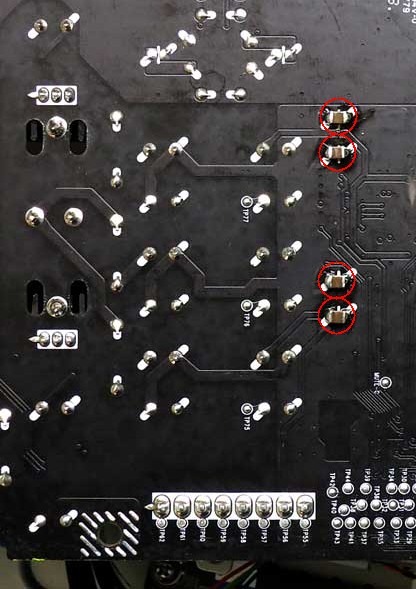
POWER SUPPLY TO POST-DAC CIRCUIT:
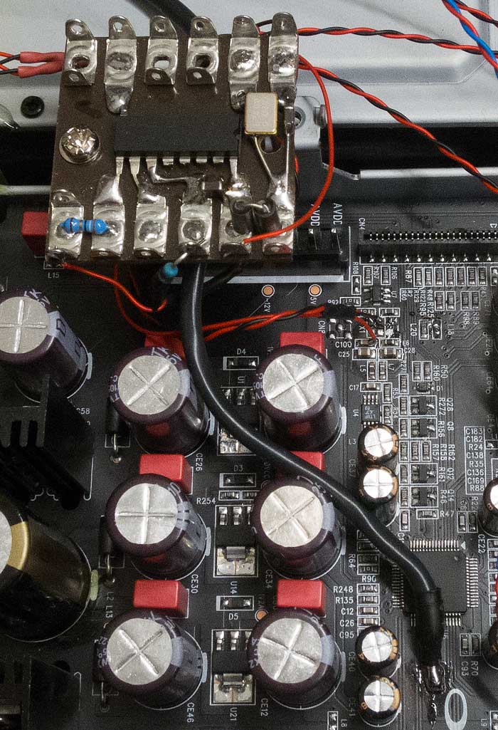
While I am using a shunt reg because the PCB I used already had them in situ, you can of course use 5V fixed regulators.
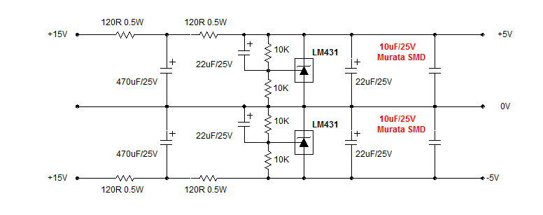
(Note: Four of the Murata caps are needed, a pair locally to each of the OPA-860.)
DC power comes from under the Stereo PCB. Please see the photo where we tap into -/+ 15V:
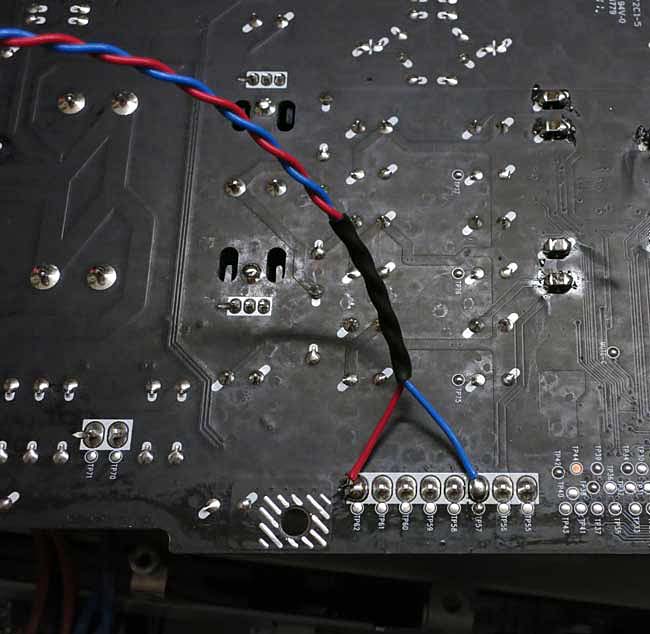
There is no 0V this is taken from here. I took this from near the DAC as a separate Ground wire. I like to use something that is similar to a Litz wire or multi-strand, so as to have near zero inductance in the Grounding.
Note there is no 0V - this is coming from near the DAC where an engraver was used to create a Ground Point:
The RCA Sockets needs to be floating.
Of course, Oppo can use their existing Ground Plane earthing.
COST: The cost is similar.
Next: Part Four
.
POWER SUPPLY TO POST-DAC CIRCUIT:
While I am using a shunt reg because the PCB I used already had them in situ, you can of course use 5V fixed regulators.
(Note: Four of the Murata caps are needed, a pair locally to each of the OPA-860.)
DC power comes from under the Stereo PCB. Please see the photo where we tap into -/+ 15V:
There is no 0V this is taken from here. I took this from near the DAC as a separate Ground wire. I like to use something that is similar to a Litz wire or multi-strand, so as to have near zero inductance in the Grounding.
Note there is no 0V - this is coming from near the DAC where an engraver was used to create a Ground Point:
The RCA Sockets needs to be floating.
Of course, Oppo can use their existing Ground Plane earthing.
COST: The cost is similar.
Next: Part Four
.
Last edited:
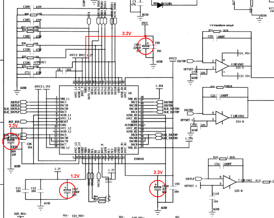
PART FOUR
SAW CLOCKING & DIVIDER:
Two clock frequencies are required and they are 54MHz for Sabre DAC (can be up to 100MHz per datasheet) and 27MHz for the "Master Clock" on the Mediatek chip. Note that they are 2:1 and that means we can use a single 54MHz SAW oscillator for direct input to Stereo DAC (and via balanced buffer drive to Multi-Channel DAC) and using a divide-by-two ship to produce the 27MHz.
Schematic:
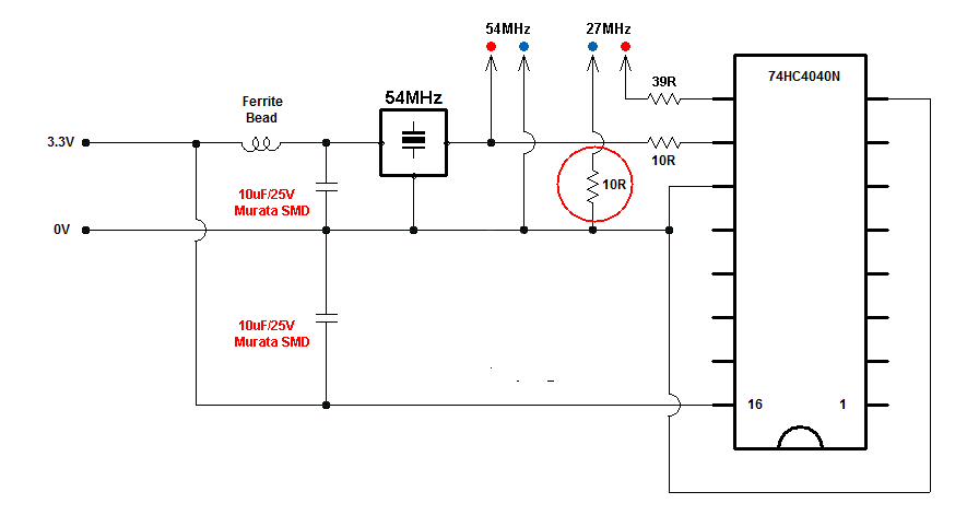
(Note that 10R in the return for 27MHz - without it you may risk increased player freezing.)
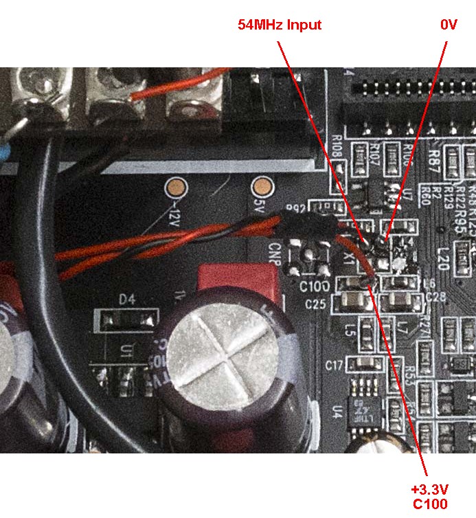
On the Oppo's Stereo Board, only the old 54MHz oscillator must be removed and three wires from above is wired to it:
As shown, we will be using the existing +3.3V clock power supply for the Sabre DAC clock after removing the existing oscillator.
How to wire the 27MHz is shown earlier on this thread.
NXP 74HC4040N (90MHz) Farnell/Element14 Part # 380-880.
Of course, Oppo could decide to use two separate SAW clocks, but they would need a decent power supply for the 27MHz and also ask Epsom Toyocom if they can make 27MHz SAWs (the lowest they have made so far is 50MHz) and if not, use 54MHz (which still has to be custom ordered like I did, but in large quantity and using two of them per player, the cost is negligible) and 2:1 divider.
Incidentally, Oppo could be attracted by the thought that we have people who say they also see an improved picture quality when using decent clocking here, rather than a cheap 27MHz Xtal. They could also order them in a smaller form factor than 7x5mm we have.
COST: The added cost, if any, is likely to be very small and possibly nil.
Next: Part Five
.
SAW CLOCKING & DIVIDER:
Two clock frequencies are required and they are 54MHz for Sabre DAC (can be up to 100MHz per datasheet) and 27MHz for the "Master Clock" on the Mediatek chip. Note that they are 2:1 and that means we can use a single 54MHz SAW oscillator for direct input to Stereo DAC (and via balanced buffer drive to Multi-Channel DAC) and using a divide-by-two ship to produce the 27MHz.
Schematic:
(Note that 10R in the return for 27MHz - without it you may risk increased player freezing.)
On the Oppo's Stereo Board, only the old 54MHz oscillator must be removed and three wires from above is wired to it:
An externally hosted image should be here but it was not working when we last tested it.
As shown, we will be using the existing +3.3V clock power supply for the Sabre DAC clock after removing the existing oscillator.
How to wire the 27MHz is shown earlier on this thread.
NXP 74HC4040N (90MHz) Farnell/Element14 Part # 380-880.
Of course, Oppo could decide to use two separate SAW clocks, but they would need a decent power supply for the 27MHz and also ask Epsom Toyocom if they can make 27MHz SAWs (the lowest they have made so far is 50MHz) and if not, use 54MHz (which still has to be custom ordered like I did, but in large quantity and using two of them per player, the cost is negligible) and 2:1 divider.
Incidentally, Oppo could be attracted by the thought that we have people who say they also see an improved picture quality when using decent clocking here, rather than a cheap 27MHz Xtal. They could also order them in a smaller form factor than 7x5mm we have.
COST: The added cost, if any, is likely to be very small and possibly nil.
Next: Part Five
.
Last edited:
PART FIVE
MURATA SMD ON DAC ETC:
Murata 10uF/25V SMD 1206 - GRM32NF51E106ZA01L - Farnell/Element14 Part # 952-7818.
These are excellent in reducing the noise floor, not just from the power supply but also the back-EMF noise that the DAC emits. DACs are essentially switching devices, and produce switching noise - this is indeed known and the DAC's manufacturers usually recommend a 100n ceramic (which we can leave in place), but that value is woefully inadequate and 10uF is actually a minimum, and electrolytics just don't cut it, for rather obvious reasons.
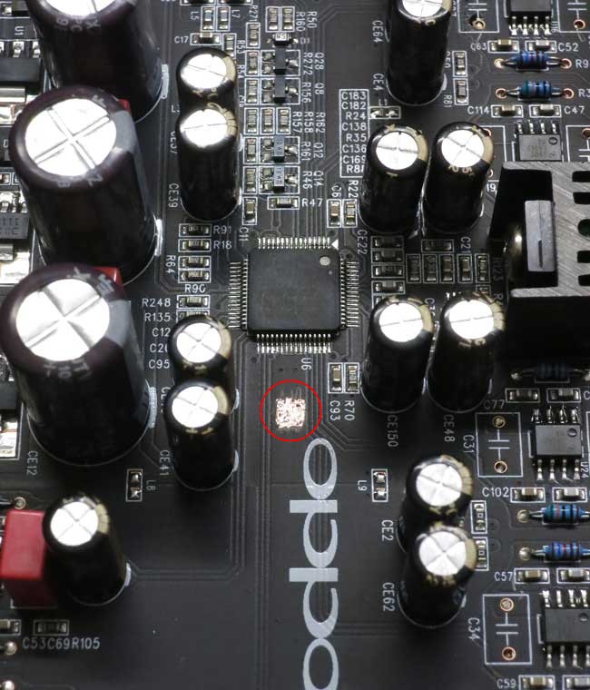
Below shows the four on the DAC.
As schematics above show, we are also using them in other areas. Right close to Pin 7 and 4 on the OPA-860 in a similar way that Oppo are using 0.47uF poly caps at the moment. Also used on the clocking and on the DAC power supply pins in same situ where Oppo are currently using electrolytics.
In total, ten will be needed. Four for two OPA-860s, four for DAC and two for the clock circuit.
COST: Not much different from equivalent electrolytic caps.
Next: Part Six - Conclusion.
.
MURATA SMD ON DAC ETC:
Murata 10uF/25V SMD 1206 - GRM32NF51E106ZA01L - Farnell/Element14 Part # 952-7818.
These are excellent in reducing the noise floor, not just from the power supply but also the back-EMF noise that the DAC emits. DACs are essentially switching devices, and produce switching noise - this is indeed known and the DAC's manufacturers usually recommend a 100n ceramic (which we can leave in place), but that value is woefully inadequate and 10uF is actually a minimum, and electrolytics just don't cut it, for rather obvious reasons.
Below shows the four on the DAC.
As schematics above show, we are also using them in other areas. Right close to Pin 7 and 4 on the OPA-860 in a similar way that Oppo are using 0.47uF poly caps at the moment. Also used on the clocking and on the DAC power supply pins in same situ where Oppo are currently using electrolytics.
In total, ten will be needed. Four for two OPA-860s, four for DAC and two for the clock circuit.
COST: Not much different from equivalent electrolytic caps.
Next: Part Six - Conclusion.
.
Last edited:
PART SIX
CONCLUSION:
I believe the above (more likely using using fixed 5V regulators), can be implemented on a new player without any hit to the bottom line.
Some final thoughts:
The R4 on the OTA is set to 10R and that means that the OPA-860 draws about 15mA each. Thought you might want to know that. The OTA is set to maximum current as 10R is virtually a short.
The R3 which set the DC on the output, this ideally should be a current source - and since about 220K can trim/null it altogether, that high Z it effectively is. The lower 15K could be split and a decoupling cap in between. But as is, it works and uses minimum number of components.
Later will try to do some distortion measurements.
I do have a fully balanced version of the above - two SOIC/OPA-860s required per channel and more symmetrical (has to be) than the above single-ended.
The single-ended unbalanced version discussed here, can also be used straight for the Multi-Channel Board - it would be a real treat.
It would be great for Coris to try the post-DAC circuit - the clocking part he is already familiar with.
I am quite pleased with the results, but won't elaborate and leave that for others to give fresh feedback and not pre-empt what they may say. Now that I have it running here, I hope to be able to play it for others in the near future.
I have done my bit - now it is up to others.
Cheers, Joe
.
Last edited:
Nice work Joe! This is a real contribution, I may say...
Just after reading your material posted here, I have two comments: I (personally) do not like long connections wires, even though it is twisted...
The other comment is about the clock frequency used. Is right that 54 Mhz it fits very well to be divided to get the clock for processor. But also the 108Mhz frequency it is dividable to get the 27Mhz clock... It is very known already that ES9018 act better (asynchronously) when about a higher clock frequency. The chip work like a charm at this 108Mhz clocking... I think one may forget such frequencies as 54Mhz, or 80Mhz...
Else, unfortunately I have stooped my work/researches on 105 (for a while), because I get very upset/angry about improvisations I faced all the time, and about quite poor equipped workshop I had. So I decided to make an real improvement in this direction before going further with Oppo 105 and some other things.
I will try for sure this idea about OTA post DAC processing, and I have to finish too, my unified clock project for this player. But, after getting upgraded my scope to 200Mhz, and put in place my new quite advanced soldering station, I have to finish also the focus servo/remote stage for my new microscope, I`m waiting for the tin feeding machines, and also I`m concentrated quite much for the time been on some many small but also important improvements in my workshop. Once those things finished it will make more easy and more productive my work in the main (modds) fields...
Last edited:
I (personally) do not like long connections wires
I agree, but for the sake of the exercise it was done this way. In principle (and in reality), the idea of generating a second clock frequency, this technique does work. As you have demonstrated too.
I doubt that Oppo would do it this way, I suspect they will stay with separate clocks/oscillators anyway. But they must get their act together and see that the 27MHz should be as important. The power supply improvement used in the '105 over the '95, for the Sabre DAC, should be at least duplicated for the 27MHz, and not just a cheap Xtal.
The other comment is about the clock frequency used. Is right that 54 Mhz it fits very well to be divided to get the clock for processor. But also the 108Mhz frequency it is dividable to get the 27Mhz clock...
We have to look at Oppo's past practices to predict what they are most likely to do.
I believe you it works, but I can assure you, as a manufacturer, Oppo is not going to use 108MHz in a new Oppo - unless of course E.E.S. can assure Oppo it can be done. But I think that in reality 1) Oppo is not going beyond the 100MHz maximum for the Sabre DAC and 2) they will most likely want to do them separately. To bring that signal down from the Stereo board would also require a balanced line driver they use for the multi-channel board, to maybe make it work. No, I can't see them doing that - they just have to make sure they get that 27MHz right with no Xtal, decent supply and may be get Epson Toyocom to make a straight 27MHz SAW (or if not, only then a divider chip with 54MHz).
I have come across a link that indicated that some other manufacturer may go as low as 30MHz, as lot closer that the lowest listed 50MHz by Epson Toyocom. Doesn't mean a quantity carrot might not interest them.
Else, unfortunately I have stopped my work/researches on 105 (for a while)...
I will try for sure this idea about OTA post DAC processing, and I have to finish too, my unified clock project for this player...
I understand. But at least I have made the effort (which means I don't have to do it again, whew!) and made it possible to get the ball rolling.
I think we should keep in mind that this goes a little beyond normal DIY and there are rules that don't apply in a more unrestricted DIY milieu, where we can do anything we feel like.
We still do our bit after Oppo has done their bit.
It will not stop us for taking it a lot further, but here the aim is to interest Oppo and perhaps slay the market and also give us something that is even further down the road where we will always add our finishing touches.
We are still not limited.
Cheers, Joe
Last edited:
Dear Joe,
many thanks for your great contribution!
While meditating your ideas, I have one question. OPA-660 is still available to buy from the Ebay. As a DIYer, I can use OPA-660. If 660 to be used, can the same schematic be used?
Sincerely appreciating for your work here,
Cheers, Seiyoung
many thanks for your great contribution!
While meditating your ideas, I have one question. OPA-660 is still available to buy from the Ebay. As a DIYer, I can use OPA-660. If 660 to be used, can the same schematic be used?
Sincerely appreciating for your work here,
Cheers, Seiyoung
I have one question. OPA-660 is still available to buy from the Ebay. As a DIYer, I can use OPA-660. If 660 to be used, can the same schematic be used?
While I am sure it can be adapted, the short answer is no. Because we have only 5V rails and critical DC as well as AC gains to target, they same component values cannot just be copied. But essentially, the idea would also work with 660. If you feel like knuckling down and do it, then you could share with us. I would certainly be as helpful as possible.
While I would have liked to go the 660 way, the point of this exercise was to use a current device and demonstrate to Oppo an alternative way. They are going to buy direct from TI, obviously not eBay. But I am sure you have already realised that.
Cheers, Joe
.
Joe, did you take measurements to verify that these modifications result in improvements?
I will be doing some measurements and they should be respectable. But will they be 'better' than the original LM4562? In what way? Static measurements don't tell the whole story - a decent measurement really only points to a credible design, not a great sounding design.
Cheers, Joe
.
I have found a thread which (by chance or not...) it were created yesterday, about OTA using in I/V stage. Some more documentation is linked there...
http://www.diyaudio.com/forums/digital-source/240987-opa861-i-v.html
http://www.diyaudio.com/forums/digital-source/240987-opa861-i-v.html
I have found a thread which (by chance or not...) it were created yesterday, about OTA using in I/V stage. Some more documentation is linked there...
http://www.diyaudio.com/forums/digital-source/240987-opa861-i-v.html
That thread was generated due to comments I made elsewhere on the OTA AD844 thread.
That thread was generated due to comments I made elsewhere on the OTA AD844 thread.
I think the same...
Output caps
> I have also set up two RCA outputs via high quality Jantzen Superior Red Z 3.3uF
> so the Silmic can be compared. My initial reaction is that the Silmic is not so shabby.
I was planning on doing something very similar. Could you comment on the difference between the Silmics and the Jantzens?
Maarten
> Could you comment on the difference between the Silmics and the Jantzens?
The Silimics are not half bad. I can understand why they are liked in outputs of digital players by manufacturers like Oppo. They take the edge of anything nasty, are nicely rounded, their shortcomings are sins of omission rather than adding anything much negative. But the Jantzen gives you warts and all, so to speak. They won't hide anything and they have the edge in transparency - but surprisingly, the Silmics don't shut down transparency totally. They are 'pleasing' sound wise.
Cheers, Joe
- Home
- Source & Line
- Digital Source
- Oppo's BDP105 - discussions, upgrading, mods...