After some searching I have discovered that B&O indeed did sell the Oppo 203 with a custom firmware and it appears there is no way of updating so yes, I will just have to live with it as is. As you say, no big improvements anyway. I just have problems with Oppo media control App freezing up and thought new firmware might solve this.
Are there coupling caps In analogue stereo outputs of Oppo 205
does anyone have a schematic of output stage
I found that my input Z was high enough that 10 mfd would be OK. I replaced the 100 polar with 10u f metallized film caps.
If you felt you needed 100u then replace the polar with bipolar type. Maybe even a film bypass.
Sorry to say that the I never got the OPPO to sound good. Even changing opamps and better couplings caps. i also removed the multi-channel output pcb. It seems to be flawed early on in the circuitry.
THx-RNMarsh
Been reading a lot on this thread, it's long but worthwhile! I have a 205, with LPS but really want the mch outputs in XLR because of my amps. Right now i use an rca to xlr converter cable but this is not optimal.. Is there a schematic on how to do this? I noticed a solution for this by Coris earlier on. Where do you take the signal and is it fully balanced?
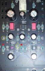
There is no schematic about such upgrade. My approach is mounting my own designed, fully balanced output modules, based on OPA1632 for the all 8 channel on board. I take the differential analog signal directly form the DAC chip outputs, dismissing the whole original post DAC circuitry. Another solution may be taking the balanced signal after the I/V converters on each channel, using parts of the original circuits. However, upgrading this section is not an easy task at all, and it is quite expensive...
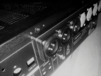
A (mechanical) challenge in implementing this upgrade, it is the mounting of the XLR connectors on the rear panel of 205. My solution is shown in the picture hereby.
A (mechanical) challenge in implementing this upgrade, it is the mounting of the XLR connectors on the rear panel of 205. My solution is shown in the picture hereby.
Attachments
I will experiment! What is a good position to obtain signal ground? Also in relation to the ground pin of the XLR.. Did you remove the RCA connectors?
- So far i've upgraded the PS capacitors to 22000uF, Kemet ALC.
- Also upgraded the main cap on my LPS from 10000uf to 22000uf.
- Also bridged the output caps for the XLR stereo outputs with a wire (my amp doesn't mind some DC) I measured only a couple of mV of DC so no problem..
- On the outputs also first tried NP black gates but they sound the same as a wire so why bother")
- I wanted to upgrade the torroid (as suggested to lightweight) but the voltages check out before and after the rectifier so i dont think this is a problem in my 205 (maybe Oppo upgraded this?)
- Ordered pos and neg regulators to replace the standard ones.
- And working on XLR outputs for the mch board. I think i will use the balanced signal after the IV going into a buffer/driver into XLR output.
Sound has improved, more natural and without output caps more detail and less harsh. So nice!
- So far i've upgraded the PS capacitors to 22000uF, Kemet ALC.
- Also upgraded the main cap on my LPS from 10000uf to 22000uf.
- Also bridged the output caps for the XLR stereo outputs with a wire (my amp doesn't mind some DC) I measured only a couple of mV of DC so no problem..
- On the outputs also first tried NP black gates but they sound the same as a wire so why bother
- I wanted to upgrade the torroid (as suggested to lightweight) but the voltages check out before and after the rectifier so i dont think this is a problem in my 205 (maybe Oppo upgraded this?)
- Ordered pos and neg regulators to replace the standard ones.
- And working on XLR outputs for the mch board. I think i will use the balanced signal after the IV going into a buffer/driver into XLR output.
Sound has improved, more natural and without output caps more detail and less harsh. So nice!
Yes, I have removed the original RCAs. There is not enough place for XLR connectors if the RCAs still be in place. A good ground for XLR on MCh is just the ground pin of the former RCA.
Concerning the original I/V circuit (isolated as described above), one should know that this is referenced to a virtual ground, which is not zero volt, but somewhere at 1,2v DC. The audio signal outputted by this I/V circuit it will be axed on this virtual ground above one volt DC. So, therefore the I/V outputs it cannot be directly connected to the XLR connectors. As usually and best is an DC offset of almost 0v for the audio signal on an output, meant for further amplification... A buffer after I/V should fix this about high DC offset. Else, AC coupling caps should be used to block the DC voltage..
Personally, I have rejected from beginning the original Oppo approach for post DAC signal processing, and I designed my own post DAC circuit.
Output pins configuration is as follow: DAC1 - pin2; DAC1B - pin3; DAC3B - pin4; DAC3 - pin 5. This configuration is symmetrical (mirrored) for all 8 output pairs pins, on both sides of the chip (all its four corners). Numeration of the "DACx/DACxB" is not important.
It seems DACx it may be the positive output, while the DACxB it may be the negative one. The differential configuration is always DACx/DACxB. Which sign on each output is less important...
It seems DACx it may be the positive output, while the DACxB it may be the negative one. The differential configuration is always DACx/DACxB. Which sign on each output is less important...
Last edited:
Can anyone give some advice on firmware upgrade for my Oppo 203 please?
I have tried to upgrade to the latest version from USB but just get a message saying 'cannot find a valid firmware upgrade file'. I have tried two different USB sticks and downloaded the file from two different laptops but with the same result.
If I try to upgrade from network I get 'cannot connect to server'
hi, Maybe I can help you with the installation of a firmware, tomorrow I try to contact you.
I discovered this page thanks to a friend and the modifications you make are amazing.
Greetings.
The B&O version is a version that I think oppo for this brand. The changes from the normal version are not significant, I think the home screen and some Infrared codes to make it compatible with your systems.
The first thing I would recommend is that you make a backup of your system. Use this script that I leave you. Unzip the file into a pendrive and insert it into the oppo on. The script will run and copy the mtd partitions of the nand memory into the pendrive. I don't think it takes more than 2 minutes.
I have found the US and AUBO versions of the firmware that you have installed, but unfortunately, I have not found the EUBO version. With the original version it would be easier to do.
To try to recreate your problem, I would need backup information to install it on my system and create a method to reinstall a normal firmware and convert it into a standard player.
There is another way to do it, but it requires a usb-ttl cable and open the player.
Attachments
D
Deleted member 537459
Hi all, great thread.
So i have oppo 203 with linear supply and 27mhz neutron star clock, i try connect a dac direct inside oppo, i take the i2s signal directly on mainboard. The dac tkae the signal and sound but i have lot distortion on high frequenze. I try many things but all i do i hve the same result. Someone try similar stuff? I see the i2s card but i need exit with all 7.1 channel.
Before i2s signal dac i mount resistor 100ohm and i
buffer the signal with 74hc245 .
Help! Thanks
thank you for your Input
did you succeed optimizing oppo 205 sound
would you please tell us what type were original AC electrolytic coupling caps and what Is your choice for 10 uF film cap
are there space to fit It
which opa did you replace I/V or differential summing
regards
did you succeed optimizing oppo 205 sound
would you please tell us what type were original AC electrolytic coupling caps and what Is your choice for 10 uF film cap
are there space to fit It
which opa did you replace I/V or differential summing
regards
I found that my input Z was high enough that 10 mfd would be OK. I replaced the 100 polar with 10u f metallized film caps.
If you felt you needed 100u then replace the polar with bipolar type. Maybe even a film bypass.
Sorry to say that the I never got the OPPO to sound good. Even changing opamps and better couplings caps. i also removed the multi-channel output pcb. It seems to be flawed early on in the circuitry.
THx-RNMarsh
Hi all, great thread.
So i have oppo 203 with linear supply and 27mhz neutron star clock, i try connect a dac direct inside oppo, i take the i2s signal directly on mainboard. The dac tkae the signal and sound but i have lot distortion on high frequenze. I try many things but all i do i hve the same result. Someone try similar stuff? I see the i2s card but i need exit with all 7.1 channel.
Before i2s signal dac i mount resistor 100ohm and i
buffer the signal with 74hc245 .
Help! Thanks
What about taking the I2S signals right from the original DAC chip I2S input, and not from the main board interface?
The I2S interface in 203 is not that simple, allowing just a tapp of the I2S components. In your case you have no any clock synchronisation. Your added DAC it cannot know what to do with the I2S signals...
By the simple tapping of the I2S from main board, you get just a mish-mash of frequencies. In 203 the digital audio dedicated to the internal DAC is fully controlled by Oppo firmware, and the necessary clock signals are synthesised accordingly by the software. The firmware and the main processor "tell" to the DAC chip how to work properly for the purpose. By simple tapping of the I2S in the way, it broke the control loop/chain for the added DAC.
In my opinion, such approach does not work. The only solution I see, is using the original DAC chip, then doing something to improve the post DAC analogue stage... Another solution it may be an reverse engineering of the original firmware, finding out how Oppo designed the control of all the things in this respect. Last solution it seems to me quite unrealistic...
D
Deleted member 537459
some people have succeeded, see vanity hd 203 which takes the signals directly from the flat cable and sends them out in spdif or directly in multichannel i2s, even oppomod has a card that picks up the signal and sends it via hdmi lvds. I thought someone had done it alone without buying something already done.
- Home
- Source & Line
- Digital Source
- Oppo new UDP series players - 203/205 - Discussions, upgrades, modifications