It's fine to use the incoming SCLK. I think if you look at my previous post more carefully you'll see what I said is the SGPIO peripheral can't generate a copy of SCLK and there's a variety of ways to deal with that should one need a copy.You can't use the incoming SCLK as SGPIO_CLK, and use the WS for synchronizing the whole stuff like for triggering the data buffer swap?
If you require a 512 Fs single speed SGPIO clock 24.5760MHz crystals and XOs are easy to get. For other situations the most cost effective way to get the clock is to use a PLL on the LPC. I would expect performance comparable to entry level clock generators but that's the sort of thing where one needs to measure the phase noise to say much that's meaningful.
Not in LPCXpresso 4.2.3 or the usual resource locations.Is there a NXP SGPIO library now, giving examples for building I2S slaves?
I2S is a low speed interface, consisting on simple shift registers. I2S has nothing to do with MCLK, and nothing to do with the audio system clock.If you require a 512 Fs single speed SGPIO clock 24.5760MHz crystals and XOs are easy to get. For other situations the most cost effective way to get the clock is to use a PLL on the LPC.
In a well designed digital audio system, by definition you never need to route a 12 MHz or 24 MHz (!) clock between the CPU and the Audio Codec, and by definition, you never need an extra PLL. Read multichannel Audio Codecs datasheets like Wolfson WM8580 or WM8581 (48 pin), or Cirrus CS42516 or CS42526 (64 pin). They all require a 12.288 Mhz quartz directly attached to them, and that's it. They feature all sorts of PLL inside (high quality with Wolfson), for avoiding to involve the CPU in the audio clock management. Such multichannel Audio Codecs love acting as I2S masters, avoiding to involve the CPU in the audio clock management.
Six months ago I was confident that NXP LPC4330 SGPIO could interface such multichannel Audio Codecs, the Codec being in Master mode.
Now, in June 2012, I'm not anymore confident about this. NXP has not released the promised SGPIO library. This is a sign that the LPC4330 may never reach volume sales. Let me tell you that when you accept exposing your precious code in an external serial Flash memory, and when you are forced to use a BGA package, you expect, as compensation, to run above 400 MHz, and possibly 600 MHz like some fast T.I. Sitara AM3358 chips (Beaglebone). On top of this, if there is the slightest indication that the LPC4330 SGPIO can't emulate a I2S slave in simplicity, that's even more fatal. Add to this the difficulty of debugging an asymetric dualcore chip like the NXP4330, and you get the full picture.
Especially when there is a gentle, simple chip like the Infineon XMC4500 in the pipeline featuring six flexible serial communication modules, each I2S-capable.
Could it be the whole LPC4330 is a hoax, only there to allow NXP selling the patented Quad SPI Flash Interface (SPIFI)? The hoax seemed to work, as NXP licenced the SPIFI to Xilinx (the Zynq-7000), and to Infineon (the XMC4500).
The day Freescale will adopt NXP SPIFI, there will be 400 MHz Cortex-M4 chips from Freescale. Same for T.I. Same for Microchip. Such move is going to change the microcontroller industry. Especially if the SPIFI content is safe, and encrypted. The microcontroller industry has not digested the 65nm design rule, and the SPIFI feature yet.
In such temporary state, let's put a few possible chips in perspective, in a modern Multichannel Audio approach.
Currently, some Microchip 100pin PIC32 chips clocked at 80 MHz feature four buffered SPI, that may be persuaded to act as 16-bit I2S without software overhead, as I2S slave. Hook a WM8580 or WM8581 (48 pin), and you are done. As those chips also feature an USB OTG, they could act as USB multichannel soundcards, if the USB software overhead stays low.
Like abraxalito wrote, you will get the STM32F372xx STM32F373xx ARM Cortex-M4 clocked at 72 MHz featuring up to three 24-bit I2S.
The Infineon XMC4500 clocked at 120 MHz is another good choice, featuring 6x Multi-function serial interface modules configurable to SPI, I2C, I2S, UART.
If you want to play with the NXP LPC4330 clocked at 204 MHz, a good choice is the LPC4330 Xplorer from NGX Technologies. It is now available from
NGX Technologies Online Store
at only $57. The documentation and examples just got updated.
Now that NXP managed to get an income stream from SPIFI, it's time for NXP to market a single core Cortex-M4 clocked at 400 MHz with 44 pin, 64pin, and 100pin (all with an extensive pin multiplex scheme), 128 kbyte RAM, equipped with six flexible serial communication modules, each I2S-capable. The unique NXP selling point would be the SPIFI allowing to load Flash code in RAM and run at full speed from RAM, at no less than 400 MHz, thanks to a 65 nm design rule. T.I. is already using the 65nm such design rule for their Cortex-M4 (LM4F series), but they cannot get them running at 400 MHz because of their slow Flash and perhaps a somewhat slow FPU implementation. The hypothetic NXP 65nm Cortex-M4 flashless chip is supposed to remain low cost, with a price about $3.50 in volume. FPU is not really needed. Such chip needs to remain low cost, for competing against T.I. Sitara AM3358 said to be $5.00 in volume. For remaining lowcost, it may be forced to drop the FPU, and the SDRAM interface. With 128 kbyte on-chip RAM, you can do lots of things in Digital Audio. If there is a single-cycle 32x32+64=64 multiplier-accumulator operating at 400 MHz, and zero-overhead loops, that's a perfect FIR engine, a perfect single-core Freescale DSP563xx killer.
Currently, ARM has no public plans about licensing Cortex-M4 MP (dual-core or quad-core) architectures in 65nm to people like NXP. If ARM goes multicore with 65nm Cortex-M4, they'll do it with Freescale. This would be a first-class DSP56K burial, and a motivation for Freescale customers to join the ARM bandwagon, while staying with Freescale. The Cortex-M4 MP dualcore feature would be welcome for executing USB-related stuff and Ethernet-related stuff, in parallel with Digital Audio.
From the NXP LPC4330, the real-world next stop is the Cortex-A8 T.I. Sitara AM3358 clocked at 275 MHz minimum like featured in Beaglebone. The AM3358 McASP needs to be studied, to determine if it can hook as I2S slave, on a WM8580 or WM8581 Multichannel Codec. Quite worrying with the AM3358, is the widespread assumption that such chip needs Linux for being able to quickly write applications for it. The AM3358, of course can run without Linux, in which case you can run without an external SDRAM. The AM3358, when used without the external SDRAM, is a very effective Digital Audio engine, and low cost. The only issues with the AM3358 are the BGA package (not easy to handle from a diyAudio perspective), and the absence of SPIFI (you need a 8-bit Flash bus and chip).
Consider processing 24-bit audio at 96 kHz, like the good old Behringer DCX2496. Consider processing six audio channels. Consider you need two moderate lenght FIRs for doing a global equalization (room equalization and psychoacoustics), plus six moderate lenght FIRs for each speaker driver. Eight FIRs in total. Consider the following FIR lenghts : 480 for the bass, 240 for the medium, 120 for the highs, and 96 as general equalizer. That's a total of 936 MACs times two for the stereo = 1872 MACs. They need to execute at 96 kHz, requiring 180 Mega MAC/s. That's just tolerable for a single-core ARM Cortex-A8 clocked at 275 MHz (like a low priced T.I. AM3358), provided the chip features a single-cycle 32x32+64=64 MAC, and zero loop overheads. It gets less critical on 65nm Cortex-M4 or Cortex-A8 clocked at 400 MHz.
With the 28 nanometer Xilinx Zynq-7000 dualcore ARM Cortex-A9 MP clocked at 800 MHz, you get more processing power. Say six 480-tap FIRs for the six speaker drivers, and two 480-tap FIR as global stereo equalizer. That's a total of 3840 MACs. They need to execute at 96 kHz, requiring 370 Mega MAC/s. And still, without needing an external SDRAM, as in the Zynq-7000, there are 256 Kbyte on-chip. There is no PowerVR™ SGX530 for 2D and 3D graphics acceleration, something you don't need in Digital Audio.
DiyAudio enthusiats will discover the merits of FIRs, shaping the impulse response at will, persuading speaker drivers to behave like they should.
The 2dB corridor from 50 Hz to 15 kHz will become the norm. System not fulfilling such norm will get disregarded. Only chips running at 400 MHz and beyond have the required capabilities.
Nowadays with low cost Android phones featuring Mediatek MT6575 1 GHz ARM processors, diyAudio enthusiasts will feel discomforted, if their Digital Audio hardware isn't in the same league. It looks crazy, it is crazy, and it's our world.
Last edited:
Oh, teh dramaz. ") Implementing section 18.8.1 of the LPC4300 manual or variants thereof isn't particularly difficult programming, loop back mode on the XMC4500 USICs has the same SCLK regeneration limitation, and a 50MHz clock is plenty in the majority of crossover and equalization cases.
Implementing section 18.8.1 of the LPC4300 manual or variants thereof isn't particularly difficult programming, loop back mode on the XMC4500 USICs has the same SCLK regeneration limitation, and a 50MHz clock is plenty in the majority of crossover and equalization cases.
Implementing section 18.8.1 of the LPC4300 manual or variants thereof isn't particularly difficult programming, loop back mode on the XMC4500 USICs has the same SCLK regeneration limitation, and a 50MHz clock is plenty in the majority of crossover and equalization cases.Oh, teh dramaz.
Really enjoyed reading your post steph - keep up the interesting theories about NXP
I'm fairly sure the TI M4 was hamstrung so that they didn't eat into their existing DSP business. Yet Steve Jobs said 'don't be afraid to cannibalize yourself'. ARM will eat their DSP business at the low end come what may, they might as well have a piece of that action. I have a couple of boards with the TI M4 (65nm) on, but this is their 'high end' part and I've been waiting for what seems like ages for them to release the cheaper, smaller package parts in the same family. I noticed on reading the datasheet they've done something weird with the SRAM - bank interleaving it looks like - before I discovered that I was hopeful the parts would be candidates for serious overclocking when running from RAM. Now, though I'm not so sure.
I think your estimates for running FIRs on A-series might be a tad optimistic. That's from experience implementing FIR on M0 - the limitation is getting the data in and out, not the MAC speed. Probably you're still thinking DSP56k where the parallel moves kept the MAC running flat out
The first 400MHz M4s might turn out to the two already inside TI's OMAP5. On the blurb I've read they didn't say what clock they would run at.
Hello abraxalito, you are right about the A-series. Is there a BDTI benchmark, specializing in FIRs? Quite demanding in FIRs, like you wrote, is the ability to move the coefficient and the data while calculating the product (on previous coefficient and data) and accumulating it, and at the same time, manage the FIR program loop without CPU cycles. No doubt a Cortex-M0 is not optimized for FIRs. A Cortex-M0 plus (still to be launched) may perform better. A Cortex-M4 is supposed to be best of all. And yes, I'm still in a doubt about the Cortex-A8, A9 and A15 as I don't know if they peform better, on FIRs, than the Cortex-M4, especially when asking the full 32x32+64=64 precision. I'm very curious about Cortex-A15 "DSP and NEON SIMD extensions onboard".Really enjoyed reading your post steph - keep up the interesting theories about NXP. I think your estimates for running FIRs on A-series might be a tad optimistic. That's from experience implementing FIR on M0 - the limitation is getting the data in and out, not the MAC speed. Probably you're still thinking DSP56k where the parallel moves kept the MAC running flat out. The first 400MHz M4s might turn out to the two already inside TI's OMAP5. On the blurb I've read they didn't say what clock they would run at.
On the other hand, there is more info available about T.I. OMAP 5 nowadays. The T.I. OMAP 5 is a ARM Cortex-A15 MP (dualcore and possibly quadcore), hyperpipelined as there are 15 stage integer and 17-25 stage floating point pipeline, with out-of-order speculative issue 3-way superscalar execution pipeline.
The ARM Cortex-A9 MP is less pipelined than the ARM Cortex-A15 MP. The ARM Cortex-A9 MP features a dynamic length, multi-issue superscalar, out-of-order, speculating 8-stage pipeline.
The ARM Cortex-A8 has a 13-stage integer pipeline and 10-stage NEON pipeline.
Viewed from a certain distance, the Cortex-A15 may turn out to be a disapointing chip, just like the Intel Pentium IV was, because of the long pipeline. Produced in old factories using a 40nm design rule, the Cortex-A15 MP would remain inexpensive, and allow smartphone vendors to apply a very appealing "1.2 GHz dualcore" on the sticker.
Worth noting is that most China Android 4.0 smartphones are now powered by Mediatek MT6575 featuring the Cortex-A9 on a 40nm design rule. This is an important milestone showing that China market is now basing on quality, instead of basing on marketing gimmicks. This will not last forever. The 32nm design rule it out there. The day the 40nm design rules gets perceived as old, there will be a possibility to reuse the same 40nm factories for producing Cortex-A15 MP chips featuring a magic "1.2 GHz dualcore" sticker or perhaps an even more ambitious "1.2 GHz quadcore" sticker. This is the practical Cortex-A15 market. T.I. is already proposing 28nm implementations, which means that the OMAP 5 market will only become significant when other vendors will announce 20nm Cortex-A9 implementations.
In parallel, modern 32nm factories will start mass production of the Cortex-A9 MP chips clocked at 1.4 GHz or so, delivering the same processing power as the 40nm Cortex-A15, while dissipating less heat. For sure, for marketing reasons, the silicon industry will always need an alternate "hyperpipelined" design, for extending the factory live cycles. I think that the Cortex-A15 and T.I. OMAP 5 turn out to be this, exactly. We'll experience the same dynamics later on when shifting from 32nm to 28nm, and later on again when shifting from 28nm to 20nm.
Here is a compilation of the available info, from T.I. OMAP 5 website, and from Wikipedia.
The OMAP™ 5 Platform. TI's first ARM® Cortex™-A15 MP mobile applications processor.
In production late 2011, to market late 2012.
Max. CPU clock rate from 1.0 GHz to 2.5 GHz
32 nm and 28 nm initially, to 20 nm roadmap
ARMv7 instruction set
1 to 4 Cores
L1 cache 64 kB (32 kB I-Cache, 32 kB D-Cache) per core
L2 cache up to 4 MB shared by all cores
L3 cache none
The ARM Cortex-A15 MPCore is a multicore ARM architecture processor providing an out-of-order superscalar pipeline ARM v7 instruction set running at up to 2.5 GHz.
ARM has confirmed that the Cortex A15 core is 40 percent faster than the Cortex-A9 core, all things being equal.
The first A15 designs taped out in the fall of 2011, but products based on the chip are not expected in the market until 2012.
Key features of the Cortex-A15 core are:
40-bit Large Physical Address Extensions (LPAE) addressing up to 1 TB of RAM.
15 stage integer / 17-25 stage floating point pipeline, with out-of-order speculative issue 3-way superscalar execution pipeline.
4 cores per cluster, up to 2 clusters per chip with CoreLink 400 (an AMBA-4 coherent interconnect). ARM provides specifications but the foundries individually design ARM chips, and AMBA-4 scales beyond 2 clusters.
DSP and NEON SIMD extensions onboard (per core).
VFPv4 Floating Point Unit onboard (per core).
Hardware virtualization support.
Thumb-2 instruction set encoding reduces the size of programs with little impact on performance.
TrustZone security extensions.
Jazelle RCT for JIT compilation.
Program Trace Macrocell and CoreSight Design Kit for unobtrusive tracing of instruction execution.
32 kB data + 32 kB instruction L1 cache per core.
Integrated low-latency level-2 cache controller, up to 4 MB per cluster.
Implementations are only expected to sample in 2011, and none are expected to market before 2012 or 2013.
Press announcements of forthcoming implementations:
Broadcom SoC
Nvidia Tegra 4 (Wayne)
Samsung Exynos 5250
ST-Ericsson Nova A9600 (Dual Core @ 2.5 GHz Over 20K DMIPS)
Texas Instruments OMAP 5 SoCs
Other licensees, such as LG, are expected to produce an A15 based design at some point.
There are two OMAP 5 devices targeted to serve different customers' needs. Both of these devices use a TI-defined, low-power 28 nanometer fabrication process.
The OMAP5430 is targeted for products such as Smartphones that demand the smallest size supporting dual-channel, LPDDR2 Package-on-Package (PoP) memory.
The OMAP5432 is targeted for mobile computing and consumer products that are more cost-sensitive, without the extreme size constraint, supporting dual-channel DDR3/DDR3L memory.
Details on the specific OMAP 5 platform components will be posted in the future.
The OMAP 5 products are intended for high-volume mobile OEMs and ODMs and are not available through distributors.
BDTI did useful architectural comparisons between Cortex-A8 and Cortex-A9, and the MIPS 74K core:
The Cortex-A9 is quite similar to the earlier Cortex-A8―both cores implement the ARMv7 instruction set architecture―but there are a few differences. Like the A8, the A9 implements a dual-issue superscalar pipeline, but the A9’s pipeline is a shorter “dynamic length” 8-stage pipe (compared to 13 stages on the Cortex-A8). In addition, the new core’s pipeline supports speculative out-of-order execution. This feature enables the processor to dynamically reorder instructions to improve performance (to avoid stalls due to instruction latencies, for example). The processor predicts which branches will be taken, and speculatively executes the code that is most likely to be chosen. This technique is used to reduce branching penalties.
Out-of-order execution is unusual in embedded processors because of the silicon cost, and it’s unusual in processors used for real-time signal processing because it increases execution-time variability. But embedded core vendors are under pressure to bump up their processing horsepower, and ARM isn’t alone in going the out-of-order route―MIPS’s new high-performance superscalar 74K core uses this technique, too.
As with the Cortex-A8, the key to the Cortex-A9’s digital signal processing capabilities is the optional NEON co-processor, which adds DSP-oriented SIMD capabilities (such as quad 16-bit multiplications) along with floating-point capabilities. If floating-point is all that’s needed, the core can be configured to include just a floating-point unit (FPU) which provides single- and double-precision floating-point capabilities. ARM has not disclosed the area required by NEON or the FPU; NEON in particular is likely to significantly increase the area required by the core. ARM also has not disclosed apples-to-apples area information for the A8 and A9, though it appears that the A9 will be smaller; previous data for the Cortex-A8 indicated that it consumes “less than 3mm^2” in a 65 nm TSMC process, excluding caches.
BDTI has benchmarked the signal processing performance of the Cortex-A8 with NEON, but has not yet benchmarked the Cortex-A9. However, it’s likely that the per-cycle throughput of the two cores will be similar on DSP tasks. Thus, the Cortex-A9’s smaller size and support for multi-core implementations are likely to be the key differentiators relative to the Cortex-A8.
The Cortex-A9 is likely to be compared to MIPS’s 74K core, which is also superscalar, synthesizable, and expected to run at 1 GHz. According to MIPS, a 1 GHZ 74K core consumes 1.7 mm^2 in a TSMC 65 nm process, excluding caches. This is slightly higher than the area ARM has reported for the base Cortex-A9 core, but such small differences are not particularly meaningful since memory usually takes up much more space on a chip than the core itself. (The addition of NEON, however, will probably increase the ARM core’s area considerably.) The MIPS 74K doesn’t have explicit hardware support for multi-core implementations, though MIPS has stated that it plans to add multi-threading capabilities to the 74K, as it did with the 34K.
As mentioned earlier, BDTI has not benchmarked the Cortex-A9 or 74K, but based on our benchmark results for the Cortex-A8 with NEON and MIPS’s estimates of the 74K’s signal processing horsepower, it appears that a Cortex-A9 with NEON will be significantly faster on typical DSP algorithms. It’s unclear how the two cores will compare if NEON is excluded.
Last edited:
hello twest820, thanks for pointing the new LPC43xx User Manual dated 8 June 2012, available here http://www.nxp.com/documents/user_manual/UM10503.pdfOh, teh dramaz.
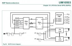
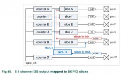
Chapter 18 starting from page 347, dedicated to SGPIO, is now more than 30 pages long.
Unfortunately, the 5.1 channel I2S proposition is unpractical. Confront it to any modern multichannel Codec. Draw the WM8581 block diagram next to it, and try connecting it. LPC43xx as I2S slave and WM8581 as I2S master. Good luck !
Attachments
Last edited:
My goodness! This discussion reminds me of my younger days when I would really get down into the low level detail of CPUs just for the fun of it. Life seems too short these days.
A £50 used PC (a quiet one) with suitable sound card provides enough computing power to implement millions of FIR taps (you don't have to emulate boring old analogue filters), provides a colourful GUI to display any info you want, allows you to develop on the actual target machine using free tools, and there's no re-sampling or jitter to worry about. What's with all the messing about with DSP boards etc.?
A £50 used PC (a quiet one) with suitable sound card provides enough computing power to implement millions of FIR taps (you don't have to emulate boring old analogue filters), provides a colourful GUI to display any info you want, allows you to develop on the actual target machine using free tools, and there's no re-sampling or jitter to worry about. What's with all the messing about with DSP boards etc.?
You may not have noticed a detail. We are dealing with realtime digital audio processing, in a high quality multichannel audio context. We assume that the nominal audio sampling frequency is 96 kHz, applied to at least six channels, each with a real 24-bit resolution. Calculate how many 32x32+64=64 multiply/accumulate you need for executing six 960-tap FIRs at the same time. You need approx 600 Mega multiply/accumulate per second. In theory, a modern PC fitted with a 5.1 USB audio attachement can do the job, possibly executing VST (Steinberg), possibly executing SynthMaker or FlowStone. Have you tried yet ?My goodness! This discussion reminds me of my younger days when I would really get down into the low level detail of CPUs just for the fun of it. Life seems too short these days. A £50 used PC (a quiet one) with suitable sound card provides enough computing power to implement millions of FIR taps (you don't have to emulate boring old analogue filters), provides a colourful GUI to display any info you want, allows you to develop on the actual target machine using free tools, and there's no re-sampling or jitter to worry about. What's with all the messing about with DSP boards etc.?
Last edited:
Calculate how many 32x32+64=64 multiply/accumulate you need for executing six 960-tap FIRs at the same time.
He already said that a silent PC could do millions of taps - you're seriously not giving him a hard enough time here steph by limiting it to six thousand
He already said that a silent PC could do millions of taps - you're seriously not giving him a hard enough time here steph by limiting it to six thousand
Yeah, the PC will implement the FIR in the frequency domain.
Note you can also do that on a DSP.
There's already a thread extant for that, but no recent activity:
http://www.diyaudio.com/forums/multi-way/20283-digital-active-xo-eq-using-pc-soundcards-brutefir.html
http://www.diyaudio.com/forums/multi-way/20283-digital-active-xo-eq-using-pc-soundcards-brutefir.html
You may not have noticed a detail. We are dealing with realtime digital audio processing, in a high quality multichannel audio context. We assume that the nominal audio sampling frequency is 96 kHz, applied to at least six channels, each with a real 24-bit resolution. Calculate how many 32x32+64=64 multiply/accumulate you need for executing six 960-tap FIRs at the same time. You need approx 600 Mega multiply/accumulate per second. In theory, a modern PC fitted with a 5.1 USB audio attachement can do the job, possibly executing VST (Steinberg), possibly executing SynthMaker or FlowStone. Have you tried yet ?
But of course you'd obviously be doing it with FFTs. You would be doing it with FFTs wouldn't you..?
Yeah, the PC will implement the FIR in the frequency domain.
Note you can also do that on a DSP.
Indeed.
Why would he do it with FFTs?
So that he wouldn't need a supercomputer to achieve precisely the same result.
If there's anyone who'd like to follow up the FFT convolution route, here's a useful starting point:
Speed Improvements
Notable is the assumption of single precision floating point for the calculations. Anyone know how the round-off noise compares when fixed point (32 or 64 bit accumulator) is used? FFT routines require sin and cos tables as look-up, also on the ARM there's no bit-reverse addressing mode which is very useful in re-ordering the output array.
- Status
- This old topic is closed. If you want to reopen this topic, contact a moderator using the "Report Post" button.
- Home
- Source & Line
- Digital Line Level
- Open Source DSP XOs