Apropos practical parasitics - or in fact anything that influences the open-loop gain & phase:
The variability of these is the whole point of considering phase margin. Phase margin is a measure of the resilience to variable circuits (and loads).
OTOH, measuring a single sample of a closed-loop design, over a few different load points, tells us only about that one sample, and those loads. It might be pure chance whether the next sample works without oscillation.
And « practical parastitics » are perfectly easily accommodated in simulations, and can be varied with ease.
.
No you can not in an easy way, short of actually getting a PCB done and measuring. Which defeats the purpose.
There exists software that reads in a PCB layout and calculates all parasitic capacitances between various traces. I was once asked to evaluate it. Neat, but iirc correctly you could only have it as a subscription. At the tune of $5k per year....
Jan
With apologies for the display order swapping about. LTSpice tends to randomly tile things.
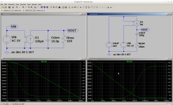
Picture 1)
Left: A simple opamp model. Dominant Pole compensation by Cdom. DC gain is 1E9/100uA. Low Frequency (DC) pole due to Rhoe with a first order, 20dB/Decade roll off with 90° phase lag.
Right: A simple Pass Device model. Current Source driving the output capacitor. A DC pole with a first order, 20dB/Decade roll off with 90° phase lag up to the ESR zero with gain becoming flat.
The graphs are the Control to Output responses. Watch out for the apparent phase inversion in the right one... the pass device acts as an inverter which is why you end up applying feedback to the positive input of the opamp.
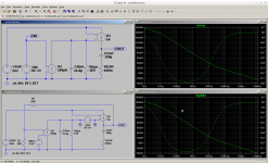
Picture 2)
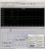
Top: The previous two models combined as a 'regulator'. 2 poles, 2nd Order, 40dB/Decade roll off with 180° phase lag up to the ESR zero becoming 1st Order, 20dB/Decade roll off with 90° phase lag at higher frequencies.
Bottom: With feedback applied.
The upper graph is the Control to Output response without feedback. Crossover is at 500KHz. The lower graph is the Loop Gain. Crossover is at 100KHz. R1 and R2 form a potential divider with a gain of 0.2 0.2 X 500K = 100K
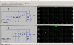
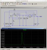
Picture 3)
Top: The previous circuit set up for a transient analysis but we run the AC analysis first.
Bottom: The previous circuit set up for a transient analysis but it is 'broken'. The gain of the pass device is reduced as is the ESR of the filter capacitor.
Upper graph shows the same response. Crossover at 100KHz with 80° phase margin. Lower graph shows Crossover at about 12KHz with effectively 0° phase margin.
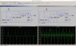
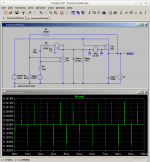
Picture 4) The transient responses of the previous circuits.
Left is stable.
Right is not.
Picture 1)
Left: A simple opamp model. Dominant Pole compensation by Cdom. DC gain is 1E9/100uA. Low Frequency (DC) pole due to Rhoe with a first order, 20dB/Decade roll off with 90° phase lag.
Right: A simple Pass Device model. Current Source driving the output capacitor. A DC pole with a first order, 20dB/Decade roll off with 90° phase lag up to the ESR zero with gain becoming flat.
The graphs are the Control to Output responses. Watch out for the apparent phase inversion in the right one... the pass device acts as an inverter which is why you end up applying feedback to the positive input of the opamp.
Picture 2)
Top: The previous two models combined as a 'regulator'. 2 poles, 2nd Order, 40dB/Decade roll off with 180° phase lag up to the ESR zero becoming 1st Order, 20dB/Decade roll off with 90° phase lag at higher frequencies.
Bottom: With feedback applied.
The upper graph is the Control to Output response without feedback. Crossover is at 500KHz. The lower graph is the Loop Gain. Crossover is at 100KHz. R1 and R2 form a potential divider with a gain of 0.2 0.2 X 500K = 100K
Picture 3)
Top: The previous circuit set up for a transient analysis but we run the AC analysis first.
Bottom: The previous circuit set up for a transient analysis but it is 'broken'. The gain of the pass device is reduced as is the ESR of the filter capacitor.
Upper graph shows the same response. Crossover at 100KHz with 80° phase margin. Lower graph shows Crossover at about 12KHz with effectively 0° phase margin.
Picture 4) The transient responses of the previous circuits.
Left is stable.
Right is not.
Attachments
OK, easily resolved:
1. start with the circuit in post 76:
Op amp Linear power supply
2. Please specify one or more of these practical parastics that can't be modelled.
So, just name a node, where some capacitance, inductance, resistance are going to make the circuit into an oscillator.
Obviously I ask you to name a realistic value of parasitic, not 100µF for the capacitance between two traces, or 300H for the ESL of a capacitor. Just name something that will overcome the 60° of phase margin that we can see in this circuit.
In Respect of Spice as a Tool.
My background is in Switch Mode Power Supplies. Various topologies up to 500W. I regularly derive idealised linear models of the design and model them in Spice. I also implement idealised switching models and model them in Spice.
It is always the case that under transient testing that the switching models match the linear models. I also get to check for component tolerances and drift over time and temperature.
It is always the case that the product on the bench behaves as predicted by the Spice models. Sometimes it seems that I have spent most of my time fixing other people's designs because they got the loop compensation horribly wrong or designed something that was marginal.
I see people who are new to Spice throwing everything including the kitchen sink into their models and then tearing their hair out because Spice sits there sulking with non-convergence errors. When it does work in Spice they build a real one and what apparently worked in Spice sits on the bench squealing at them or decides to self destruct.
The opto-isolator has a 5:1 variation in current transfer ratio. They used a wire-wound resistor for current limiting. They tried to operate a current sense transformer at 100% duty cycle. They forgot or did not know about the Right Half Plane Zero in their Flyback Converter. They hit an 'edge case' when things just wobble about.
All of a sudden Spice gets a bad name because the user messed up or did not use it judiciously.
And yes. My Switch Mode Power Supplies are somewhat benign in terms of loop bandwidth but I still have to pay a great deal of attention as to how I lay out the circuit boards and implement other components in order to achieve low output noise and EMI.... and loop stability.
I have little to no doubt that the same is required in terms of PCB layout when you arbitrarily drop 80MHz Gain-Bandwidth Product Operational Amplifiers into a circuit that, closed loop, might only achieve a bandwidth of 100KHz and end up listening to The Police, not the band, because you did not apply local feedback and have to resort to putting your circuit in a Magic Biscuit Tin.
Last edited:
OK, easily resolved:
1. start with the circuit in post 76:
Op amp Linear power supply
2. Please specify one or more of these practical parastics that can't be modelled.
So, just name a node, where some capacitance, inductance, resistance are going to make the circuit into an oscillator.
Obviously I ask you to name a realistic value of parasitic, not 100µF for the capacitance between two traces, or 300H for the ESL of a capacitor. Just name something that will overcome the 60° of phase margin that we can see in this circuit.
I didn't say they can't be modeled - please don't put words into my mouth. I said you don't know them before you layout the PCB.
Yes, you can assume some values and design the circuit so that it is robust against those values. But still you must have some idea of the values à priori.
All I was saying that it isn't 'a shame that xxx is ignored'. MF is obviously an expert. Many here are what the forum is about: diyaudio. Measuring a build-up circuit with a simple means like a square wave on the ref and looking at Vout is practically within anyone's reach, easily interpreted and can be used as a base for tweaking.
I am not going to have this blown into a full-scale war about measuring methods; I believe I have been clear and you can have the last word because you cannot resist that ;-)
Jan
Yes, you can assume some values and design the circuit so that it is robust against those values. But still you must have some idea of the values à priori.
Jan
This is the exact reason why SPICE is valuable with this kind of design work.
If your circuit models with near zero phase margin (as some circuits here do), you are probably wasting time building and testing it with square waves (or any other method).
First, you have to compensate it properly. If you don't do this, it is only a matter of chance whether your circuit will work with a given load, or a given sample-set of components. Checking with load-steps is only valid for the prototype you built, and the conditions you tested, and maybe even only the temperature range you tested it in. With the first component swap or load beyond the tested range, the user is at risk of failures.
I suspect that many DIYers will see the value in doing better than that.
Measuring a build-up circuit with a simple means like a square wave on the ref and looking at Vout is practically within anyone's reach, easily interpreted and can be used as a base for tweaking.
Jan
If you can generate signals, and have a oscilloscope, you can measure phase margin almost as easily.
The only one extra you need for this: some kind of isolating transformer. A small OT from an SE amplifier will be perfect, or failing that, simply pick up a 9-15V low voltage mains transformer. The transformer does not have to have flat frequency response, because you are going to measure relative values.
Method:
1. Break the loop in the positions shown in the SPICE diagrams (MordbidFractal conveniently labels these as A and B). Wire the SECONDARY winding into this break. The B node should have relatively high impedance, for most-accurate working.
2. Drive the mains winding with a signal generator. The signal should be small: just enough to measure on the scope will suffice.
3. Measure A and B simultaneously on the 2-channel scope.
4. Recording some frequency points will allow the creation of a bode plot.
5. When the two signals are equal, you're at the crossover, or 0dB frequency... The phase shift here allows the phase margin to be assessed simply by observation.
The difference between measuring phase margin - and simply changing parts until the circuit stops oscillating - is obvious. At least, it is once you grasp the principles of frequency compensation.
And if you start with a circuit that has been frequency-compensated in SPICE first, you will find that the work often goes very well, and predictably.
I didn't say they can't be modeled - please don't put words into my mouth. I said you don't know them before you layout the PCB.
But you are talking about nH/inch or pF/inch^2. That might matter at RF but then you have to use RF capable components in your circuit and operate them as RF capable components if you need to care. Of course since you do... you do. If you did not then you would not.
Yes, you can assume some values and design the circuit so that it is robust against those values. But still you must have some idea of the values à priori.
Only if you want to put RF capable components in your circuit and by design or mistake expect or discover that they are going to operate as RF components. Of course you might consider stopping them being RF capable by design.
All I was saying that it isn't 'a shame that xxx is ignored'.
Fine by me. I hope that xxx feels the same.
MF is obviously an expert.
My Conservative Councillor doorstepped me. I asked him about the #IPAct. He went 'blah'. I explained to him how it suffered from various flaws. He turned to his colleague and suggested that I was an 'expert'.
According to you, and at least one other, I presume to 'Speak The Truth'. Someone else has said.. "please don't put words into my mouth." Who was that? Why do it to me?
No.. I am not an expert. I just have some experience of these things. I can, do and will get some of it wrong. I do not mind if I am called for it.
Many here are what the forum is about: diyaudio. Measuring a build-up circuit with a simple means like a square wave on the ref and looking at Vout is practically within anyone's reach, easily interpreted and can be used as a base for tweaking.
Might not be the best choice. As per Mooly. If you do not have access to a B&K, Billion Kroner, or HP, Huge Price, programmable load you can knock one up with a Mosfet and your signal generator.
Picture 1) as per previous. Crosses over at about 12KHz. Unstable at 12KHz. And no... it might be easily interpretable if you know but it is not suitable for tweaking if you don't. It just tells you where something might be wrong.
Anecdote. Someone else's supply used a MagAmp to pre-regulate a linear post regulator. Technician looked at the load transient response and expressed a concern. I sucked teeth and agreed... Not part of my remit. Other, in charge, Engineer says it is within specification so it goes into production and falls over.
Everyone else is flapping about the place so I stick my nose in on the sidelines and change R1 and C1 on the MagAmp feedback loop whilst burbling why at the Technician who called the problem in the first place and got ignored...
I am not going to have this blown into a full-scale war about measuring methods;
I don't think anyone was 'going to war' on measuring methods. ISTM we were talking about Loop Stability.
I believe I have been clear and you can have the last word because you cannot resist that ;-)
Jan
Toys.. Pram... Bloke takes broken football back. Sorry I could not resist the opportunity to fullfil your last word prophecy.
Attachments
It's a shame to see MorbidFractals excellent practical demonstrations of reliable oscillation-free power & control loops ignored like this, in favour of arbitrary methods of stability testing.
Closing the loop around an op-amp-driving-a-power-transistor without checking the phase margin is like flying blind.
A circuit may appear to be stable at first measurement, but all kinds of things that affect the open-loop gain (temperature, sample-to-sample variation of transistors, load current, reactive loads etc etc) are likely to change in real life, and between one person's build and another.
Unchecked, uncompensated designs are highly likely to go bad a some point.
But if your circuit has, say 40-90° of phase margin, you can build with more confidence - and preferably do some practical testing.
Of course you have to check the small-signal stability, and that definitely has to include checking that the circuit is not at the edge of instability, but in my opinion whether you do that by checking phase margin, small-signal step response or any of the other available methods is completely irrelevant. I mean, your 40 to 90 degrees of phase margin is just as arbitrary a criterion as striving for less than 20 % overshoot and no ringing in the small-signal step response.
In fact, for a second-order system with the main compensation zero in the input to output transfer, like some of Mooly's circuits, 65 degrees phase margin, 21 % overshoot in the closed-loop step response, Butterworth closed-loop pole locations and a broad peak of 2.08 dB in the small-signal closed-loop transfer are all essentially equivalent. When the main compensation is in the feedback path, 65 degrees phase margin, 4 % overshoot in the closed-loop step response, Butterworth closed-loop pole locations and maximally flat small-signal closed-loop transfer are all essentially equivalent. Just measure or simulate whatever criterion you find most convenient to measure or simulate. As the thread starter has no sine wave source, measurements based on step responses should be the most convenient for him - unless he also has no 'scope, of course.
By the way, none of the methods for checking small-signal stability can guarantee large-signal stability. Applying large steps and checking whether the circuit recovers is the only method I know of to check that.
Last edited:
I mean, your 40 to 90 degrees of phase margin is just as arbitrary a criterion as striving for less than 20 % overshoot and no ringing in the small-signal step response.
Designing for a phase margin of 40-90° is not an arbitrary target. Not at all. Ensuring that our loop does not rotate phase by 180° at the crossover is the stability criterion, with 40-90° margin as a realistic target that should usually be achievable, and it is sufficient to account for all the usual variations that affect every circuit made from disparate components.
Perhaps it would be better if I say 'Design and Test for Phase Margin' rather than 'checking for phase margin' because the design portion of the work is at least as important as the testing.
You may choose to test by examining overshoot, but what happens when the result is borderline, or if it fails? Sooner or later you are going to have to consider phase rotation, in order to apply frequency compensation.
I draw attention to this question of phase margin because otherwise, the impression given to would-be circuit designers or constructors is that it's OK to design a composite voltage-regulator and then stabilise it by swapping & adding components until the problem appears to go away. And I am certain that there are always DIYers and other visitors to the site who wish to do better than that - and learn how to design and develop properly.
Since the SPICE representation of the circuit is less than 100% accurate, I find that I seldom get exact matching between (simulated phase margin & measured phase margin). By the same token, I seldom get exact matching between (simulated risetime & measured risetime), and also (simulated transient overshoot & measured transient overshoot).
One reason for this is: my estimates (guesses!) of parasitic capacitances on the actual hardware, and installed into SPICE, are not always perfect. Another reason is: SPICE modeling of power MOSFET gm vs Ids, is not always perfect. (Whereas, BJT SPICE modeling of gm vs Ice is generally excellent). A third reason is: the ESR and ESL of real electrolytic capacitors, are not always identical to the SPICE model. A fourth reason is: the discrete compensation capacitor in a "Miller" arrangement, is connected to the same nodes as several semiconductor junctions. The capacitance of these junctions, vs bias voltage and bias current, is not always identical to the SPICE model.
For these and other reasons, I seldom get the exact measurements that I expected from SPICE simulations. So I tinker around with the compensation components, to see whether (a) I'm very close to a Cliff Of Death; (b) I can get the results that SPICE predicted; (c) I can get results better than what SPICE predicted.
As viewed by a disinterested third party, what appears to happen is: (i) bare PCBs arrive; (ii) components are stuffed and soldered; (iii) the board is connected to test equipment and measurements are made; (iv) component values are tweaked and twiddled while more measurements are made; (v) when tweaking and twiddling (during measurements) is complete, the job is done. Exactly what some people recommend NOT doing.
Designing for a phase margin of 40-90° is not an arbitrary target. Not at all. Ensuring that our loop does not rotate phase by 180° at the crossover is the stability criterion, with 40-90° margin as a realistic target that should usually be achievable, and it is sufficient to account for all the usual variations that affect every circuit made from disparate components.
Perhaps it would be better if I say 'Design and Test for Phase Margin' rather than 'checking for phase margin' because the design portion of the work is at least as important as the testing.
You may choose to test by examining overshoot, but what happens when the result is borderline, or if it fails? Sooner or later you are going to have to consider phase rotation, in order to apply frequency compensation.
I draw attention to this question of phase margin because otherwise, the impression given to would-be circuit designers or constructors is that it's OK to design a composite voltage-regulator and then stabilise it by swapping & adding components until the problem appears to go away. And I am certain that there are always DIYers and other visitors to the site who wish to do better than that - and learn how to design and develop properly.
If you like to use phase margins to establish how close to small-signal instability your circuits are, that's fine with me. It is a good method, especially for simulations and calculations. For measurements it adds some overhead; for example, what impact will the parasitics of your transformer have? Still, if you can keep that under control, that's all fine. If you want to advocate the use of phase margins on this forum, by all means, please go ahead.
However, your repeated use of the word "properly" annoys me in your posts. It implies that Jan, Mooly and I are doing it improperly, which in my opinion is simply not correct. I can assure you I have designed dozens of feedback amplifiers that were produced in millions without ever calculating, simulating or measuring a phase margin and without ever getting a single customer complaint about them.
What I did do is look at small- and large-signal step responses, closed-loop frequency responses and for the more complex cases, root loci and pole-zero extractions. For active filter synthesis I usually just calculate the transfer function without worrying about whether there are any feedback loops in the circuit.
To answer your question, when the overshoot of the small-signal step response is excessive or when you see excessive ringing or even oscillations, you can for example estimate or simulate where the main poles and zeros of the loop gain are, draw a root locus and see from the root locus plot what you can do to reduce the Q of the closed-loop pole pairs. Simulations of the small-signal step response (or of the closed-loop pole locations, when you have a pole-zero extractor) can then show you if the expected improvement also occurs when second-order effects are taken into account, to the extent that the simulation covers these. For cases that occur frequently, like simple second-order systems with a zero, you only have to draw the root locus once in your life, after that you know what the possible ways to reduce the Q are.
Of course all of this is equivalent to increasing the phase margin. That's just the point: there is a whole bunch of methods to analyse feedback loops that are essentially equivalent to each other, and are therefore to my opinion equally proper.
When possible, it is wise to also check recovery from large steps and weird initial conditions once the small-signal step response is OK. That may be difficult in reality, but it's easy to do in simulations.
However, your repeated use of the word "properly" annoys me in your posts. It implies that Jan, Mooly and I are doing it improperly, which in my opinion is simply not correct.
Have you posted any circuits for Regulators in this thread? I don't remember seeing any. If not, I can't be suggesting you're presenting any 'improper' design work. The others can speak for themselves, if they are as easily 'annoyed' as you are.
If you are using analysis and measurement using whatever techniques you like, and arriving at solutions where the stability criterion is satisfied - meaning that a suitable phase margin is achieved, then naturally, I have no quarrel with you. If you feel that your methods to achieve this aim are more suitable for the problems of this low-voltage regulator, feel free to advocate them too.
No, but I did make some comments on the stability of proposed regulators and suggested that the thread starter should measure the small-signal step response to determine stability. The reason why I suggested using the small-signal step response is a very pragmatic one: he simply doesn't have the equipment to measure phase margin.
Anyway, I'm glad we agree now.
Anyway, I'm glad we agree now.
Let's Go Boutique.
Someone else... I'll fail to properly quote Lloyd Dixon from Unitrode but having mentioned his name I must, obviously, be correct suggested that,
For certain flavours of Switch Mode Power supplies the loop is designed to crossover, first order, at some frequency determined by the topology. The final answer is unknown, it is constrained by the circuit, but calculations can be made.
The zero frequency is set to be half of the crossover frequency. The pole frequency is set to be twice the crossover frequency. The phase margin at crossover becomes 45°. Apparently this results in 'critical damping'.
The OP has suggested all these poles and zeros are confusing and the maths possibly even more so. I feel the pain and I may not be helping especially when I try presenting sums... or blithering on about poles and zeroes.
Anyway.
It seems we want to use Boutique Wide Bandwidth OpAmps and Boutique Zero ESR output capacitors and in order to do so we have to tweak our 'real life' circuits on the bench until they seem to work.
Picture 1) A Boutique Wide Bandwidth Operational Amplifier Spice Model.
I've already given that one. In this case I've just increased the input stage current by a factor of 10 to hit a 10MHz Gain Bandwidth Product.
Picture 2) The previously suggested regulator model with a Boutique Zero ESR filter capacitor.
This time I have added local feedback around the Boutique Operational Amplifier. E1 is there to isolate the feedback node.
Guess What... I, interactively with some intuition, tweaked the component values to get the final result. Nominally First Order at crossover with 'about' 45° phase margin. I am a criminal.
Picture 3) The transient response.
Picture 4) Zoom In... Critical Damping, no Over or Under Shoot. I guess, unlike me, Lloyd Dixon knows something.
Someone else can provide or introduce the opportunity to, within reason, discuss the caveats.
If you want to play start out by setting E1 to 0V.
...
Attachments
-
 Screenshot at 2018-01-17 14:48:53.png42.1 KB · Views: 117
 -
 Screenshot at 2018-01-17 14:45:04.png42.5 KB · Views: 128
 -
 Screenshot at 2018-01-17 14:41:19.png50.5 KB · Views: 121
 -
 Screenshot at 2018-01-17 14:11:18.png48.5 KB · Views: 123
 -
opamp10MHz.asc1 KB · Views: 36
-
acboutique.asc3.1 KB · Views: 41
-
transient04.asc3.1 KB · Views: 39
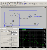
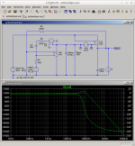
OK, you seem to know what you are talking about.
Can you educate me? See attached, one of my designs. From this graph I conclude it is stable, what with sufficient phase margin. Yet, it oscillates. Why, what am I not getting?
How should I modify this bode curve to make it stable?
Jan
Can you educate me? See attached, one of my designs. From this graph I conclude it is stable, what with sufficient phase margin. Yet, it oscillates. Why, what am I not getting?
How should I modify this bode curve to make it stable?
Jan
Attachments
OK, you seem to know what you are talking about.
Can you educate me? See attached, one of my designs. From this graph I conclude it is stable, what with sufficient phase margin. Yet, it oscillates. Why, what am I not getting?
How should I modify this bode curve to make it stable?
Jan
It very much depends on what you have measured in order to get that plot. There is mention elsewhere in the thread of perturbing the reference and measuring the output voltage.
Picture 1) Notice that I have set VAC to 0V and applied the AC excitation to the reference. Then I plot the output voltage. Apart from the absolute amplitude, 13dB vs 50dB, the curves seem to follow what you have given.
This is the input to output response. In your case there appears to be more abrupt gain peaking.
Picture 2) As before I have broken the loop with VAC and plot V(a)/V(b) in order to get the loop gain. Mr Coleman has suggested a method for doing this sort of measurement on real circuits...
http://www.ti.com/lit/an/snva364a/snva364a.pdf
Picture 3) I can, in part, mimic what you are seeing by forcing the zero, CP smaller in conjunction with RF, in my circuit to higher frequencies but your phase plot is suggesting there is something else going on prior to crossover.
I could try to mimic that but it would be a guess as to what might be going on and what is causing it. Wet finger would say your pass device is having problems prior to the operational amplifier giving up.
Looking at the scaling and given you are a man that knows how to make measurements I might take a guess that this is some sort of High Voltage, 50dB = 300V, regulator.
Rumour has it that as long as crossover occurs with sufficient phase margin your circuit will be stable.
Unfortunately Murphy's law says that if for some reason your circuit can get into a state where its overall gain drops to a level where crossover occurs with little to no phase margin it will choose to do so and oscillate.
It is the difference between conditional and unconditional stability and the nature of the phase shift in your circuit indicates that Murphy is likely to be paying a visit.
For my sins I really cannot comment much further. Perhaps you might like to provide the actual circuit so I can poke about with it in Spice.
Attachments
<snip> .. and the nature of the phase shift in your circuit indicates that Murphy is likely to be paying a visit.
Yes, with the phase shifting 100° in 2 octaves around the crossover, it would not take much deviation in parameters (between model and real circuit) for the phase margin to vanish.
Example: Voltage headroom in the pass transistor (i.e. regulator dropout) would strongly affect device capacitances - especially with FETs, and thus the location of its associated pole.
Probably have to settle for lower closed-loop bandwidth in the finished design, which should be fine for most analogue audio loads. The actual approach to frequency compensation depends on the circuit, as MF says.
MF, Rod, thanks for the replies, appreciate it. Two confessions: 1) this is not a regulator but a (high voltage) linear amplifier, and 2) I may be someone who knows how to do measurements*, but all this poles and zero stuff, while I understand the concepts, is hard to grasp and apply for me.
I need some time to digest this.
Jan
*the plot I showed was from LTspice.
I need some time to digest this.
Jan
*the plot I showed was from LTspice.
- Status
- This old topic is closed. If you want to reopen this topic, contact a moderator using the "Report Post" button.
- Home
- Amplifiers
- Power Supplies
- Op amp Linear power supply